
8 - Inspection and test techniques
8.3 - In-circuit and functional test
Functional test
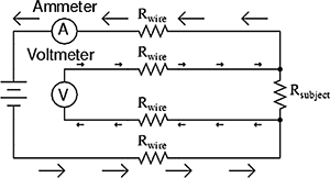
To check the electrical functions of the circuit modules after assembling, in-circuit and functional tests are made. With in-circuit test, the electrical connections of the components and the PCB are checked. Functional tests are aimed to try the functions of the final product: the module is driven with power source and the signals are monitored. A basic method for accurate measurement e.g. of resistances is the 4-wire resistance measurement, which is a very simple measurement setup and gives very accurate measured values. To avoid including the resistance of the measurement wires into the measureable value, four wires are used. A measurement current is driven through the subject and the voltage is measured just between the two terminal points of the measureable resistance. With this, very low current is flowing through the wires of the voltmeter (because of the high inner resistance), so the voltage drop on them is negligible. Knowing the flowing current and with measuring the voltage, the resistance of the subject can accurately be determined.
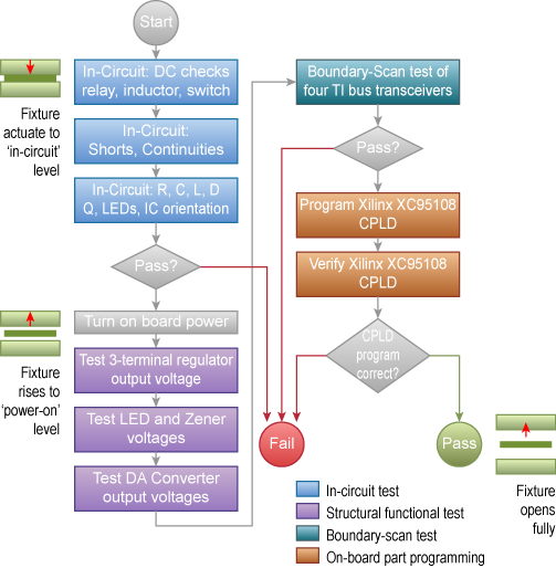
In-circuit tests (ICT) mainly measure simple parameters, like resistance (value checking, short-circuit or breakage detection), polarity of components (diode, capacitor), voltage, current. Functional tests are more sophisticated, determining amplification, transfer function, signal level, etc. of analogue and digital circuits. The circuit firstly goes through the ICT session, then if passed, the functional test session comes next. After this, comes the boundary scan of the complex ICs, then might come the programming of PLDs (Programmable Logical Unit). Boundary scan is a method for testing the functions of assembled FPGAs, ASICs and processors via their Test Access Ports. With special test vectors, the IC can be driven, data be read from its inputs. To be able to do this, the designer has to insert special test cells, latches for this purpose to the in- and outputs. With these, the parts of the circuit can be examined independently. Thorough these ports, the IC can be driven with special test vectors, and the output data checked. This method provides a very fast testing even at high complexity advanced circuits.
ICT probes
The in-circuit tester is based of some pins fixed or able to move in X-Y dimension, which contact the dedicated special pads or holes on the PCB. These measuring points are specially designed according to the DfT (Design for Testing) rules. In-circuit test equipment consists of two main parts. The first is the tester itself. This consists of a matrix of drivers and sensors that are used to set up and perform the measurements. There may be 1000 or more of these driver sensor points. These are normally taken to a large connector conveniently located on the system. This connector interfaces with the second part of the tester - the fixture. In view of the variety of boards this will be designed specifically for a particular board, and acts as an interface between the board and the in circuit tester. It takes the connections for the driver sensor points and routes them directly to the relevant points on the board using a "bed of nails".
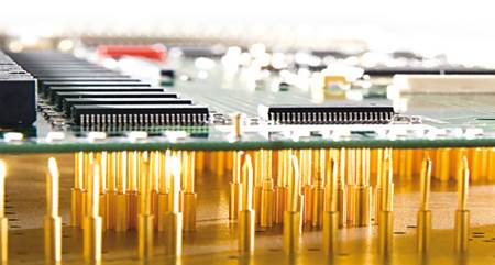
In order to carry out the test it is necessary to gain access to each node on the board. The most common way of achieving this is to generate a "bed of nails" fixture. The board is held in place accurately by the fixture and pulled onto spring loaded pins that make contact with connections on the board. The board may either be pulled down under the action of a vacuum or it may be achieved mechanically. At one time when board component densities were much lower it was often possible to place special ATE pads onto the board to enable good connection to be made. Nowadays with very much more compact boards this is not possible. Instead connections are made onto the component pads. This is obviously more difficult because of the solder and the component connection itself, but can still be achieved to a high degree of reliability. Typically each spring exerts a force of between 1–2 N to ensure that good contact is made. This obviously means that the total force required for all the pins on a board can be very significant. Sometimes supports for the board are required to ensure that it does not bend too much as this may result in cracking some delicate surface mount components. Typically pins are placed on a 25.4 mm matrix. Many new surface mount IC packages require a much finer pitch, and to achieve this an adapter is often used.
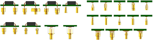
There is a great variety of different types of pin that can be used. The major design changes are within the head or tip that contacts the board under test. Each type of head has a particular application for which it is best suited. Concave tips may be used to connect onto terminal posts, flat tips or those with a spherical radius may be used to connect onto card edge fingers, whilst those with a sharp point may be used to connect onto component pads. These sharp tips will penetrate any oxide layer, giving a high level of reliability on soldered areas. The different styles of measurement tips: crown, spear, chisel, blade, convex, concave, flat etc. The wiring in the fixtures is generally not neatly loomed together. Whilst this may not be as aesthetically pleasing, it reduces the levels of cross-talk and spurious capacitance. It also reduces the wire lengths within the fixture as the shortest route between two points can be taken within reason.
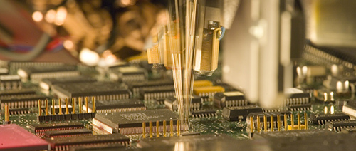
Flying probe testers
The Fixtureless in-circuit test (FICT) or Flying probe (FP) test is a cost-effective and flexible method. It is used with low to medium volumes. A program automatically recognizes the test pads by an AOI and moves the flying probes in X-Y-Z direction to the accurate position. The number of pins reaching the board at the same time is programmed. The pins can reach the PCB by multiple angles. This is useful at fine-pitch devices. It is very cost-effective with low volumes, because it is flexible: if testing a new circuit, only the program has to be changed. To maintain the best contact resistance, the pins have to be carefully checked from time to time. The probes and the fixtures have to be very carefully checked to avoid false measurement results and avoid board damage.
Advantages of a flying probe test system:
- No special fixture required – in view of the fact that the probes move according under software control to make contact with the required nodes, the "bed of nails" fixture required for ICT is not required. SA simple generic mechanism to hold the board in place is needed.
- Changes can be made easily – as the probes move under software control, any changes to pad positions or components can be made by purely changing the software. It is not necessary to make any mechanical changes to a fixture as in the case of a "bed of nails" fixture.
- Test development time reduced – software for a flying probe tester can be developed relatively quickly from the PCB design files. The big saving is that no mechanical fixture is required and its manufacturing time is not needed. Accordingly development of the test program for the flying probe tester simply requires the PCB files, and ultimately a first off board or boards on which to test the program.
Disadvantages of a flying probe test system:
- Speed of operation is slow – when compared to other forms of automated test equipment such as an ICT, the flying probe tester is much slower because the probes have to physical move to each position in turn. For an ICT system all the connections are in place in the fixture.
- It may not always possible to make complicated tests – Using early flying probe testers it was not possible to test components beyond passive components or diodes. To achieve higher levels of fault detection technologies such as boundary scan and the use of on-board memory enable more complicated tests to be undertaken. It is necessary to check the performance of the individual flying probe tester to ensure it can meet the requirements.
| Previous | Next |