
6 - Wave soldering and thermal profiles
6.1 - Process steps of wave soldering, process parameters
Process of wave soldering
Wave soldering is a large-scale soldering process by which electronic components are soldered to a printed circuit board (PCB) to form an electronic assembly. The name is derived from the fact that the process uses a tank to hold a quantity of molten solder; the components are inserted into or placed on the PCB and the loaded PCB is passed across a pumped wave or Waterfall of solder. The solder wets to the exposed metallic areas of the board (those not protected with solder mask), creating a reliable mechanical and electrical connection. The process is much faster and can create a higher quality product than manual soldering of components. Wave soldering is used for both through-hole printed circuit assemblies, and surface mount ones. In the latter case, the components are stuck by adhesive onto the printed circuit board surface before being run through the molten solder wave.
As through-hole components have been largely replaced by surface mount components, wave soldering has been supplanted by reflow soldering methods in many large-scale electronics applications. However, there is still significant wave soldering where SMT is not suitable (e.g. large power devices and high pin count connectors), or where simple through-hole technology prevails (certain major appliances).
As through-hole components have been largely replaced by surface mount components, wave soldering has been supplanted by reflow soldering methods in many large-scale electronics applications. However, there is still significant wave soldering where SMT is not suitable (e.g. large power devices and high pin count connectors), or where simple through-hole technology prevails (certain major appliances).

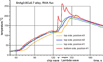
The temperature experience of the wave soldered joint, the „profile” typically shows a steady temperature rise to over 100 °C, then a rapid rise to a peak of 240–250 °C at the time of solder immersion. The fact that a large quantity of liquid metal is present to transfer heat is a key difference between wave soldering and reflow soldering, and one that explains the lack of a stabilization plateau (soak) region.
Process parameters of wave soldering
Some basics to start / check the parameters for a wave soldering machine are listed below. Explanation of the technical terms such as "Dwell time, solidification time and wetting time is also given.
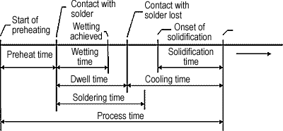
Preheating
The temperature of the board (component side) during preheating should rise as quick as possible to 45 °C (with maximum slope of 2 °C/s) and just before soldering to the temperature of 85 °C.
The temperature of the board (component side) during preheating should rise as quick as possible to 45 °C (with maximum slope of 2 °C/s) and just before soldering to the temperature of 85 °C.
Wetting time
The duration between the moment of first contact (between the components to be soldered and the solder) and the moment that the solder achieved complete wetting.
The duration between the moment of first contact (between the components to be soldered and the solder) and the moment that the solder achieved complete wetting.
Dwell time
The duration between the moment of first contact (between the components to be soldered and the solder) and the moment of last contact with the solder. This duration should be between 2 and 4 seconds.
The duration between the moment of first contact (between the components to be soldered and the solder) and the moment of last contact with the solder. This duration should be between 2 and 4 seconds.
Soldering time
The duration between the board actually contacts the solder and the onset of solidification. Dwell time + approximately 5 to 10 seconds
The duration between the board actually contacts the solder and the onset of solidification. Dwell time + approximately 5 to 10 seconds
Solidification time
The duration that the solder is getting solid on the bottom of the board.
The duration that the solder is getting solid on the bottom of the board.
Cooling time
Forced cooling after soldering reduces the maximum temperature reached in the areas on the component side of the board. However, forced cooling directly after the dwell may cause unequal shrinkages, which will initiate cracks and therefore not advised. If rapid cooling down is needed, the best place of cooler fans will be before or in the lift itself.
Forced cooling after soldering reduces the maximum temperature reached in the areas on the component side of the board. However, forced cooling directly after the dwell may cause unequal shrinkages, which will initiate cracks and therefore not advised. If rapid cooling down is needed, the best place of cooler fans will be before or in the lift itself.
| Previous | Next |