
3 - Solder paste stencil printing
3.1 - Stencil manufacturing technologies
Solder paste deposition
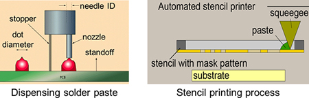
The solder paste can be applied in two ways to the pads; by dispensing or by stencil printing. Due to its productivity stencil printing is the method for mass applying solder paste, where a squeegee forces the paste through the apertures to pads in one step. Dispensing is slower process because the paste is applied to pads one by one, therefore this method is used mainly at prototyping. Its advantage is that a relatively expensive stencil is unnecessary.
Chemical etching
Stencil manufacturing methods include three technologies; chemical etching, laser cutting and electroforming. All technologies have advantages and disadvantages, which should be taken into account when choosing stencil for given application.
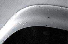
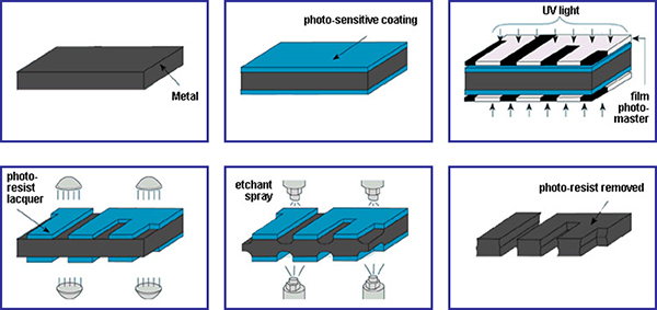
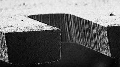
Chemical etched stencils are the workhorses of the stencil world. They are the most cost effective and the quickest to turn around. (Same day shipments are a daily occurrence.) Chemical etched stencils are created by coating a metal foil with resist, exposing an image onto both sides with a pin-registered photo tool and then etching the foil from both sides simultaneously using a dual-sided process. Since the process is dual-sided, the apertures, or openings, are created as the etchant works through the metal not only from the top and bottom, but also horizontally. Inherent in this technique is the creation of a knife edge, or hourglass, configuration. While at 0.5 mm pitch and under, such a profile presents an opportunity for paste adherence into apertures.
Properties of chemical etched stencils:
- Subtractive technology, cheap
- Hour-glass shape aperture, material is brass
- Appropriate for pitch size >0.63 mm
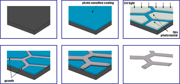
The steps of chemical etching are the followings:
- Chemically clean the surface of the metal to be etched
- Apply photo sensitive coating to both top and bottom sides
- Develop the photo resist usually solving it by UV light
- Rinse off the photo resist
- Etch the metal from both sides simultaneously
- Complete etched product
Lasercut stencils
Produced directly from the customer's original Gerber data, laser-cut stainless-steel stencils feature an absence of photographic steps. Hence, eliminating the opportunity for misregistration. A stencil can be made with excellent positional accuracy and reproducibility. The Gerber file, after the necessary modifications, is transferred to (and directly drives) the laser. Less physical intervention means fewer opportunities for error. Although there were initial concerns about the dross (vaporized molten metal) created by the laser beam, the current generation of laser cutters produces minimal dross that is removed easily. The major drawback of the laser-cut process is that the machine cuts each aperture individually. Naturally, the more apertures, the longer it takes and the more costly the stencil. The laser technique is the only process that permits an existing stencil to be reworked, e.g., to add apertures, enlarge existing apertures or add fiducials.
Properties of lasercut stencils:
- Subtractive technology, medium cost
- Trapezoidal aperture, material is nickel or stainless steel
- Appropriate for pitch size >0.4 mm
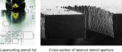
A trapezoidal aperture may be used to enhance solder paste release. In chemical etch processes, the trapezoidal dimension, Z, can be specified. At lasercut process trapezoidal apertures are created automatically per the laser beam's focus, which aids paste release. The apertures actually are cut from the contact side of the stencil, the stencil then is flipped and mounted with the squeegee side up.
Electroform stencils
Electroforming creates a nickel stencil with a unique gasketing feature that reduces solder bridging and minimizes the need for underside stencil cleaning. This process provides near-perfect registration with no geometric limitations, smooth vertical side-walls with a built-in taper and low surface tension to enhance paste release. The stencil is created by imaging photoresist on a substrate where the apertures are intended and then plating - atom by atom, layer by layer - the stencil around the resist to the desired thickness. During the process the nickel atoms are deflected by the photoresist to create a trapezoidal configuration. Next, when the stencil is removed from the substrate, the top becomes the contact side to create the gasketing effect. A continuous nickel thickness range of 25 to 300 µm may be selected. This process is ideally suited for ultra-fine-pitch requirements (0.2 to 0.4 mm). As for drawbacks, since a phototool is involved (albeit one-sided) the potential for misregistration exists. And if the plating process is not uniform, the gasketing effect is negated.
Properties of electroform stencils:
- Additive technology, expensive
- Material is nickel
- Appropriate for pitch size >0.15 mm
The steps of electroforming are the followings:
- Clean the metal substrate, which is usually nickel
- Apply photo sensitive coating
- Developing and rinsing off solved photo-resist
- Deposit metal by electroplating around the photo resist
- Remove photo resist and separate the stencil foil from the substrate
- Complete electroformed stencil
| Previous | Next |