
6 - Wave soldering and thermal profiles
6.2 - Wave soldering equipment
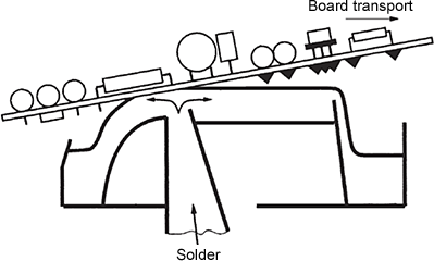
Parts of the wave soldering machine
The main parts of a wave soldering machine are the fluxer, pre-heater and the solder bath – solder wave.
Depositing flux
There are two methods for depositing flux onto the bottom side of the PCB in wave soldering. These are the foam fluxing and spray fluxing. For either flux application method, precise control of flux quantities is required. Too little flux will cause poor joints, while too much flux may cause cosmetic or other problems.
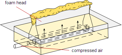
The foam fluxer consists of a tank of flux into which a plastic cylinder with tiny holes is immersed; this is sometimes called a "stone". The plastic cylinder is covered with a metal chimney. Air is passed through this cylinder which causes flux foam to rise up the chimney, forming a cascading head of foam. As the PCB passes over the foam head, flux is applied to the PCB.
The foam fluxer consists of a tank of flux into which a plastic cylinder with tiny holes is immersed; this is sometimes called a "stone". The plastic cylinder is covered with a metal chimney. Air is passed through this cylinder which causes flux foam to rise up the chimney, forming a cascading head of foam. As the PCB passes over the foam head, flux is applied to the PCB.
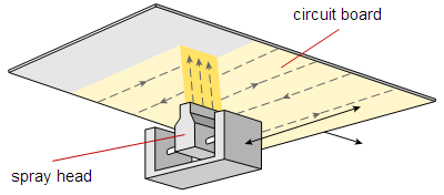
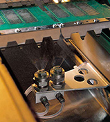
Spray fluxers consist of a robotic arm which travels from side to side while spraying a fine mist of flux onto the bottom side of the board. Some spray fluxers consist of a stationary bar with a series of nozzles that spray a fine mist. There are also additional ones that can consist of a single stationary ultrasonic head and/or an oscillating ultrasonic head. Some systems will then use compressed air to remove excess flux or to completely remove flux from some areas.
 |
 |
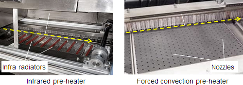
Pre-heating
A freshly fluxed board cannot be wave soldered successfully unless its underside has been heated to a temperature of about 100°C, the exact temperature depending on the flux being used. The reasons for preheating a board are:
- To evaporate volatiles
- To start flux activation
- To reduce thermal shock on the assembly when dwelling
- To meet the "thermal demand" of the assembly
Solder bath
Wave soldering is usually the best method to use when high throughput rates are required. The single wave soldering (Omega wave soldering) principle is the most straightforward method and can be used on simple substrates with two-terminal SMD components. More complex substrates with increased circuit density and closer spacing of conductors can pose the problem of non-wetting (open joints) and solder bridging. Bridging can occur across the closely spaced leads of multi-leaded devices as well as across adjacent leads on neighboring components. Non-wetting is usually caused by components with plastic bodies. The plastic is not wetted by solder and creates a depression in the solder wave, which is augmented by surface tension. This can cause a shadow behind the component and prevent solder from reaching the joint surfaces.
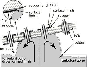
During the soldering process, the following interactions start at the onset of contact between the assembly and the solder wave:
- Point of entry, which is the most dynamic part of the wave since the directions of board travel and solder flow are in direct opposition to one another. This differential motion creates a washing action that removes the flux from the board, and will also flush away organic layers such as any surface contamination.
- Component leads on other side need to be soldered, and plated through holes must be wetted and filled with solder. The hole filling is primarily produced by wetting taking place between solder and metallization and the resulting surface tension forces: capillary action ensures that solder will rise up the holes.
- Point of exit (peel back)
To estimate the hole filling during single-wave process, the expression for capillary action may be used. When a capillary tube is placed in a liquid, such as water, a concave meniscus forms. Adhesion occurs between the fluid and the solid inner wall pulling the liquid column up until there is a sufficient mass of liquid for gravitational forces to overcome these intermolecular forces. The height of the liquid coloumn is expressed by:
where is the liquid–vapor interfacial energy, is the wetting angle, is the density of the liquid (solder), is the standard acceleration due to gravity, is the inner radius of the capillary tube. This expression can be extended to estimate the hole filling at through-hole components. In this case, the force due to the surface tension acts on two perimeters (component lead and plated through-hole), and the weight of the liquid coloumn can be calculated as a weight of a tube.
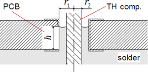
Writing the balance of forces (surface tension and gravitational):
where is the inner radius of the plated through-hole, and is the radius of the component lead. Rearranging this to make the height of the liquid coloumn the subject:This expression implies that insufficient hole filling can occur when using thick PCBs (e.g. above 2 mm), or the difference between the inner radius of the plated through-hole and the radius of the component lead is large.
For wave soldering of surface mount assemblies and complex through-hole assemblies, two solder waves (Double wave soldering) are used. The first solder wave (Chip wave) is usually a fast flow-rate, turbulent wave formed by some mechanical means. It is formed by pumping the solder through rows of small fixed or moving holes at the outlet of the nozzle or by means of a unidirectional hollow jet wave. The jet wave's flow trajectory is usually aimed in the same direction as the board's travel direction. The turbulent action of the first wave causes the solder to move in and around all the chip components to help ensure that all solder joints get soldered. This ensures good solder contact with both edges of the components and prevents joints from being missed. The first turbulent wave is followed by an asymmetrical laminar, slow flow-rate wave (Lambda wave). The second smooth laminar wave completes the formation of the solder fillet, removes excess solder, and prevents bridging.
Board handling
There are two methods of holding PCB assemblies in the conveyor:
- Fixtures (or ‘pallets’, or ‘templates’, or ‘carriers’), which may be adjustable or made specifically for a particular board profile.
- Finger conveyors, which hold rectangular boards by the edges and are adjustable only in width.
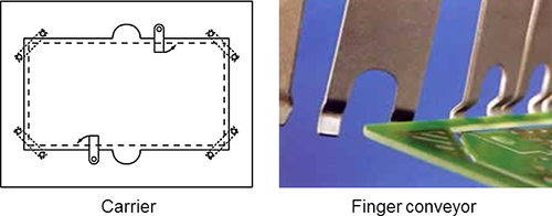
If a finger conveyor is too tight, the boards may have a tendency to bow as they are going over the wave solder bath. This phenomenon occurs when the finger conveyor is too tight and, as the board goes up through the system, it wants to expand. Since there is not enough room for this expansion, the board bows down into the wave solder pot, creating a change in the contact area with the wave, which also changes the dwell time in the solder, impacting the soldering of the board. Defects typically found due to this situation are indicators something is not correct in the conveyor operation. These defects include:
- Icicles on the bottom side
- Solder source side shorts
- Solder balls on the solder source side
- Shallow hole fills on outer edges of the board
- Missing solder on outer edges of the board
- Excess solder on the trailing edge of the topside of the board
| Previous | Next |