
6 - Wave soldering and thermal profiles
6.4 - Selective (wave) soldering
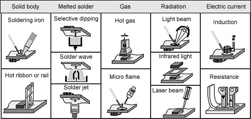
Types of selective soldering according to the heat transfer medium
Selective soldering is the process to selectively solder components to printed circuit boards, molded modules, etc. that could be damaged by the heat of a reflow oven in a traditional surface mount technology (SMT) assembly process. This process usually follows an SMT reflow soldering process and the devices to be soldered are through-hole mounted connectors or similar large components. The devices to be selectively soldered are surrounded by components that have been previously soldered, and the selective solder process must avoid these components to be damaged. The selective soldering processes are usually categorized according to the heat transfer methods and tools. The soldering can be made by:
- A hot solid body, called soldering iron
- Melted solder, which can be a miniwave, can be delivered by stamps, or can be a solder wave touched by the board through a masking pallet
- Gas, either in the form of hot gas, or of burning gas, that is a gas flame
- Heat induced by electric induction
- Heat transferred by radiation of either Infrared light or a laser beam
- When collective soldering methods cannot be used
- For rework of soldering defects
- For soldering at non-accessible places or components
- With solders of different melting temperatures
- For heat sensitive boards or devices, and so on
Selective wave soldering methods
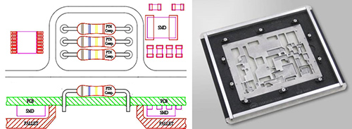
Selective wave soldering by applying mask
Over a solder wave, selective soldering can be carried out by using aperture tooling. The tools, named pallets, effectively mask off the areas populated by previously reflow soldered surface mounted components. They allows also the soldering of plated through hole (PTH) components to dual sided mixed technology assemblies where there are apertures in the tool. Through the apertures of the pallet the wave gets in contact with the board where there are terminations of the through-hole components not soldered yet. The pallets have machined pockets to protect solder side surface mount devices (SMD) and shield the heat and solder from thermally sensitive or non-glued parts. The PCB assembly with the pallet is then passed over traditional wave soldering equipment to complete the process. Each tool is specific to a PCB assembly, i.e. each board needs individual mask.
Over a solder wave, selective soldering can be carried out by using aperture tooling. The tools, named pallets, effectively mask off the areas populated by previously reflow soldered surface mounted components. They allows also the soldering of plated through hole (PTH) components to dual sided mixed technology assemblies where there are apertures in the tool. Through the apertures of the pallet the wave gets in contact with the board where there are terminations of the through-hole components not soldered yet. The pallets have machined pockets to protect solder side surface mount devices (SMD) and shield the heat and solder from thermally sensitive or non-glued parts. The PCB assembly with the pallet is then passed over traditional wave soldering equipment to complete the process. Each tool is specific to a PCB assembly, i.e. each board needs individual mask.
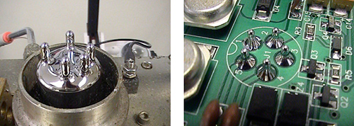
Selective soldering by solder wetted stamps
At selective soldering by solder wetted stamps, the melted solder is delivered by a tool of special shape, named stamp, to the leads of the through-hole components. There are cavities on the top face of the stamps of prism forms. After dipping into and then lifting out the stamps from a solder bath, solder remains in the cavities and it raises out forming a liquid bump that is suitable to make soldering. The PCB is placed above the stamps with the liquid solder bumps and all leads in the printed circuit board are soldered simultaneously when the stamps get in touch with the PCB. Each tool is specific to a given product.
At selective soldering by solder wetted stamps, the melted solder is delivered by a tool of special shape, named stamp, to the leads of the through-hole components. There are cavities on the top face of the stamps of prism forms. After dipping into and then lifting out the stamps from a solder bath, solder remains in the cavities and it raises out forming a liquid bump that is suitable to make soldering. The PCB is placed above the stamps with the liquid solder bumps and all leads in the printed circuit board are soldered simultaneously when the stamps get in touch with the PCB. Each tool is specific to a given product.
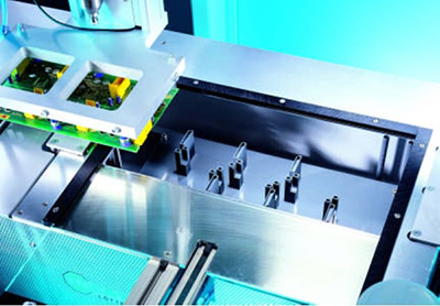
Mini wave soldering: with a miniature solder fountain
Miniature wave selective solder fountain(s) typically use a miniature pumped solder wave with a spherical shape similar to the end of a pencil to sequentially solder the PCB. The small wave gets in contact with the board on a small spot, where soldering takes place. With the mini wave leads can be soldered individually. Moving the solder spot along a line, e.g. the pin row of connectors can be soldered. This process is somewhat slow, but very accurate. The PCB may be fixed and the wave/wave solder pot moved underneath the PCB in 3-axis, or alternately the PCB may be articulated over a fixed wave/solder bath to perform the selective solder process. This process is generally regarded to be tool-less. Multi-nozzle soldering heads and nozzles with gap outlet openings are also in use to fasten the process and to reduce cycle time.
Miniature wave selective solder fountain(s) typically use a miniature pumped solder wave with a spherical shape similar to the end of a pencil to sequentially solder the PCB. The small wave gets in contact with the board on a small spot, where soldering takes place. With the mini wave leads can be soldered individually. Moving the solder spot along a line, e.g. the pin row of connectors can be soldered. This process is somewhat slow, but very accurate. The PCB may be fixed and the wave/wave solder pot moved underneath the PCB in 3-axis, or alternately the PCB may be articulated over a fixed wave/solder bath to perform the selective solder process. This process is generally regarded to be tool-less. Multi-nozzle soldering heads and nozzles with gap outlet openings are also in use to fasten the process and to reduce cycle time.
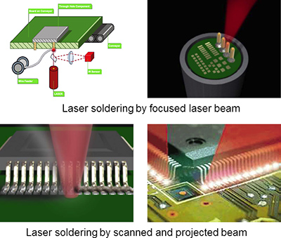
Laser beam soldering
A laser soldering system usually uses a solid state laser with near infrared wavelength, like the Nd:YAG lasers. The beam is delivered to the leads or components either by deflecting the beam or by positioning the assembly. General advantages of laser soldering includes:
- The application of small spot size with the required diameter or shape, which results in exact heated area and low effect to the surrounding areas and parts
- Very high intensity of the laser beam, therefore the heating can be very fast, which results in short processing cycle and energy efficient soldering
- Programmable processing, no need for tools specific to a PCB assembly
| Previous | Next |