
5 - Reflow soldering ovens and reflow profiling
5.2 - Thermal profile measurement and reflow failures
Reflow profiling
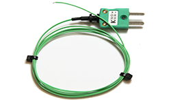
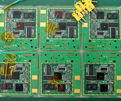
Reflow profile measurement is a vital part of setting up reflow solder conditions. The measurements are typically carried out using thermocouples attached to a high temperature resistant recording device which travels through the reflow oven with the PCB under test. Special care must be taken to ensure proper placement of thermocouples to accurately measure temperature at the desired locations. Accessories for thermal profiling are: thermocouples, data register, data processing software.
 |
 |
Thermocouples (TCs) for the measurements should be placed in joints expected to be the warmest and coolest, so that the range of peak temperatures for all components on the board can be confirmed to be within specifications. The warmest joints on a board are typically belongs to small passive components; so one of these should be monitored for peak temperature on the profile board. The coolest joints on a board are typically belongs to large BGAs and sockets. A TC should be used in a joint at one corner of the component, and in a joint at the center of the device, or as near to the center of the device as possible. Sockets with actuating mechanisms may require an additional TC at a joint near the mechanism, if its mass could make that area harder to heat. In addition to solder joints, component body temperature, measured at top center or as close as possible, may also needed to be monitored, to avoid exceeding the body temperature spec of the device.
Reflow failures
Low peak temperature
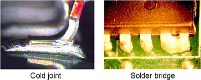
With lead-bearing alloys (Sn63Pb37), the coolest joints on board should reach at least 210 °C. With SAC305 or SAC405 lead-free alloys, the coolest joints on a board should generally reach at least 228 °C, preferably 235 °C. For the lead-free alloys, the temperature 228 °C represents smaller than 10 °C superheating above the initial melting point (219-221 °C). The 235 °C represents 15 °C superheating. Temperatures lower than these can result in joints that are not fully formed, or form in reduced quality and reliability as cold joints. Low peak temperature generally causes bad wetting, open joints or even solder bridges.
With lead-bearing alloys (Sn63Pb37), the coolest joints on board should reach at least 210 °C. With SAC305 or SAC405 lead-free alloys, the coolest joints on a board should generally reach at least 228 °C, preferably 235 °C. For the lead-free alloys, the temperature 228 °C represents smaller than 10 °C superheating above the initial melting point (219-221 °C). The 235 °C represents 15 °C superheating. Temperatures lower than these can result in joints that are not fully formed, or form in reduced quality and reliability as cold joints. Low peak temperature generally causes bad wetting, open joints or even solder bridges.
High peak temperature
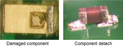
250 °C is recommended as the maximum temperature for all solder joints on the board, except for components with temperature ratings lower than 250 °C. If maximum solder joint temperatures exceed 250 °C, PCB damage such as delamination and warpage may result when standard FR4 (Tg =130 °C) material is used. Higher Tg material is not necessarily more resistant to this damage, and must be tested for compatibility. Components are typically rated as per J-STD-020C (or later), based on their package thickness and volume. Although Intel BGAs are generally rated at 260 °C, other components, especially large ones, may be rated at 250 °C or 245 °C. This means that 250 °C may not be usable as the maximum joint temperature for some components; a lower temperature may be required. Since larger components normally reach lower maximum temperatures during reflow than smaller ones, because of the different heat capacities, keeping them below their ratings may not be difficult, as long as 250 °C is used as the maximum temperature for the joints of smaller components. High peak temperature can cause the damage of the component, damage of the assembly or detach of the pervious soldered components.
250 °C is recommended as the maximum temperature for all solder joints on the board, except for components with temperature ratings lower than 250 °C. If maximum solder joint temperatures exceed 250 °C, PCB damage such as delamination and warpage may result when standard FR4 (Tg =130 °C) material is used. Higher Tg material is not necessarily more resistant to this damage, and must be tested for compatibility. Components are typically rated as per J-STD-020C (or later), based on their package thickness and volume. Although Intel BGAs are generally rated at 260 °C, other components, especially large ones, may be rated at 250 °C or 245 °C. This means that 250 °C may not be usable as the maximum joint temperature for some components; a lower temperature may be required. Since larger components normally reach lower maximum temperatures during reflow than smaller ones, because of the different heat capacities, keeping them below their ratings may not be difficult, as long as 250 °C is used as the maximum temperature for the joints of smaller components. High peak temperature can cause the damage of the component, damage of the assembly or detach of the pervious soldered components.
Short soak time
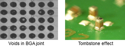
Short soak time can cause high temperature differences on the assembly (large ΔT in peak temperature), voiding in the joints, which is especially critical in BGA packages, skewing & tombstoning.
Short soak time can cause high temperature differences on the assembly (large ΔT in peak temperature), voiding in the joints, which is especially critical in BGA packages, skewing & tombstoning.
Fast ramp-up rate
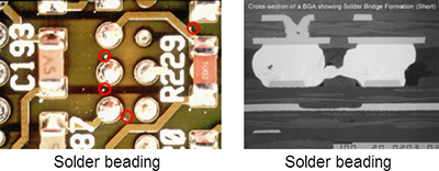
To avoid component damage, manufacturers often recommend that the rate of temperature increase during heating (Rising Ramp Rate) and cooling (Falling Ramp Rate) be kept below 3 °C/s. This applies throughout the heating and cooling process. Fast ramp rate can cause either poor wetting or solder beading.
To avoid component damage, manufacturers often recommend that the rate of temperature increase during heating (Rising Ramp Rate) and cooling (Falling Ramp Rate) be kept below 3 °C/s. This applies throughout the heating and cooling process. Fast ramp rate can cause either poor wetting or solder beading.
Cooling rate
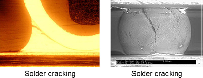
During cooling from peak temperature down to 205 °C, it is recommended that a falling ramp rate between 1.5–5 °C be used. Solder joints formed with cooling rates of 1°C/s or greater are characterized by finer microstructure features. Literature studies indicate that this is better for long term reliability. Faster cooling rates inhibit growth of intermetallic compounds in the bulk solder and can cause cracking of solder joints.
During cooling from peak temperature down to 205 °C, it is recommended that a falling ramp rate between 1.5–5 °C be used. Solder joints formed with cooling rates of 1°C/s or greater are characterized by finer microstructure features. Literature studies indicate that this is better for long term reliability. Faster cooling rates inhibit growth of intermetallic compounds in the bulk solder and can cause cracking of solder joints.
| Previous | Next |