
3 - Assembly of electronic circuits
3.2 - Assembly of through-hole components
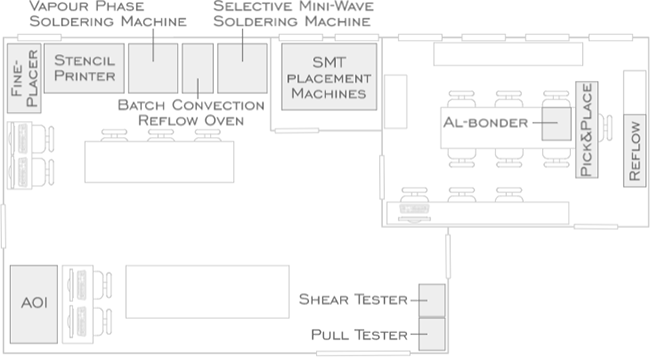
Floor-plan of the assembly laboratory
Wave soldering
After placing the TH components, depositing the flux and preheating the assembly, the mass soldering technology is wave soldering for Through-Hole assemblies. In double wave soldering, the first, so-called Chip wave is a turbulent, fast flow velocity wave, which provides the necessary amount of solder to the soldering pads and forces the solder into the narrow plated-holes in the PWB. The second, so-called L (lambda) wave is laminar, slow flow velocity wave, which removes excessive solder and eliminates solder bridges.
Selective wave soldering
In mixed assemblies, the surface mounted components are assembled by reflow soldering technologies, while the through-hole components can be soldered by selective wave soldering. Selective means that soldering is taking place locally. A pump presses melted solder through a nozzle, thus a small spherical solder wave is formed on its outlet. The liquid solder is protected from oxidation by nitrogen gas flowing out from the surrounding cylinder. The PCB is fixed, while the soldering head is positioned and moved beneath the through-hole leads.
Pin-in-paste technology
In mixed assemblies, the through-hole components can also be assembled by pin-in-paste technology. In the case, both the through-hole and the surface mounted components are soldered by reflow soldering technology. The only difference is the apertures are opened in the stencil for through-hole components as well.
| Previous | Next |