
1 - Virtual Laboratory Support for Microelectronics Packaging Education
1.1 - Introduction to the course
Course objectives
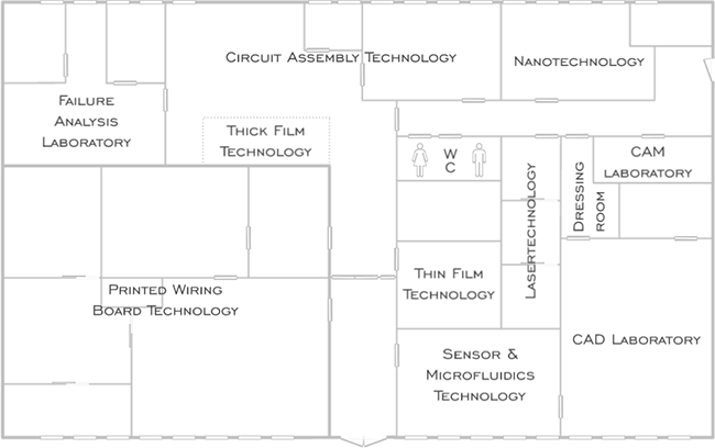
The objective of the course “Virtual Laboratory Support for Microelectronics Packaging Education” is to provide an overview about the content and usage of a virtual laboratory focusing on microelectronics packaging. The virtual laboratory includes brief descriptions about the basic principles of different packaging technologies, about the equipment and manufacturing machines related to the packaging technologies, and also animations about the principles of manufacturing processes and about the operation of manufacturing machines. The virtual laboratory covers the following areas of microelectronics packaging: manufacturing of printed wiring boards; assembly of electronic circuits – soldering technologies; nanometrology, sensors & microfluidics technology; thin-film and thick-film technologies; laser technologies; failure analysis.
Target students
BSc and MSc students with knowledge of physics, material science, electronics
Learning outcomes
- Knowledge: the students will be acquainted with the principles of the processes of electronics packaging technologies. The students will know the operating mechanism of machines in the manufacturing line, and will be able to analyse the machines’ basic specifications.
- Skills: the students will be capable to make a distinction between different packaging technologies (e.g. thick-film, thin-film, PCB based) and to relate the proper equipment and infrastructure for these technologies.
- Competences: the acquired competences allow the students to analyse machines operating in the electronics production, and to provide aid for design engineers during the stages of designing, purchasing and building manufacturing lines for electronic products.
Developed by
Budapest University of Technology and Economics, Department of Electronics Technology
| Previous | Next |