
2 - Manufacturing of printed wiring boards
2.3 - (Electro)chemical technologies
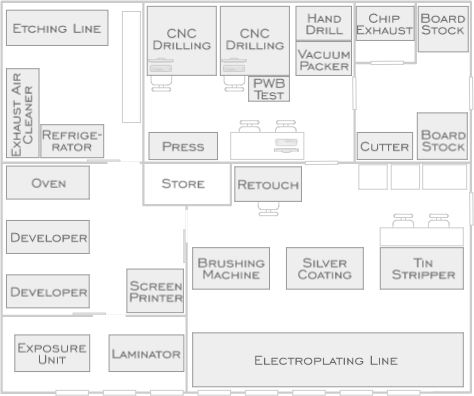
Floor-plan of the PCB laboratory
Electroplating
Electroplating technologies are used for through hole plating and pattern plating on PCBs. The electroplating process contains several chemical steps such as cleaning, surface preparing, plating of various metals, etc. All these steps are organised in one equipment line.
Etching
The unnecessary copper will be removed by etching from the board surfaces that are not covered with Sn pattern mask. The most important components are: Etching section for removing copper, washing section for cleaning the board from etching chemicals and a drying section.
Tin stripping
The stripper machine removes the tin layer (Metal Etch Resist) from the etched printed wiring board. It works using more spraying nozzles, filled by various chemicals. These materials dissolve the tin. Residues of chemicals are removed by high-pressure water spraying.
Screen sprinting of solder mask
The basic tools used in printing are the squeegee and the screen. The system that incorporates these basic tools and provides adequate means for controlling them precisely in the fabrication is the screen printer. The holes of the polyester, or nylon screen are free and there is a window on the screen made by using special masking tape, according to the PCB size. The PCB is placed under the screen and the squeegee presses the soldermask ink through the screen while traveling along.
Surface finishing - immersion silver
| Previous | Next |