
6 - Technology of printed wiring boards
6.1. Manufacturing technologies of single and double sided printed wiring boards (PWBs)
Printed Wiring Boards (PWBs)
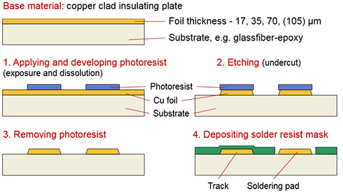
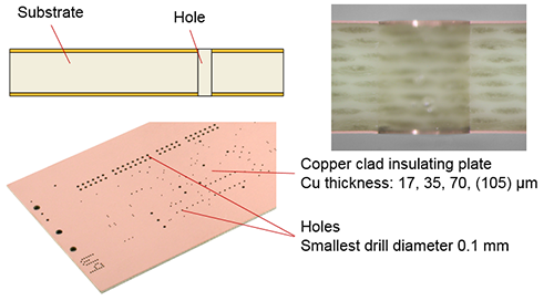
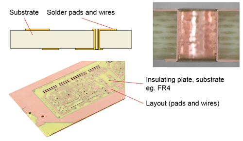
Printed Wiring Board: A conductor layout (wiring) is created on an insulating resin substrate, the conductive metal is usually copper, thickness: 17, 35, 70, (105) µm.
Function: Electrical connections among components' pins and mechanical fixing of components.
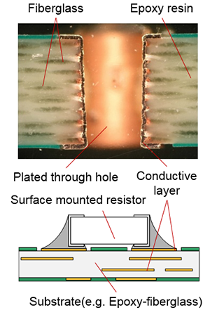
Features: Mechanical properties of substrates (rigid, flexible, rigid-flex). Number of conductive planes (single- and double-sided, multilayer). Processing technology (subtractive, additive, semi-additive)
Substrates of PWBs:
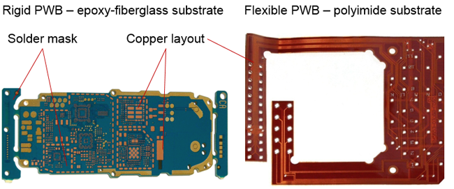
Rigid substrates: Reinforcement: paper, fiberglass, polyaramide, metal. Resin: phenol, epoxy, polyimide, PTFE – polytetrafluoroethylene (Teflon)
Flexible substrates: epoxy, polyester, polyimide, PEN – polyethylene- naphthalate, PTFE
Flexible substrates: epoxy, polyester, polyimide, PEN – polyethylene- naphthalate, PTFE
Properties of substrate materials:
| Resin | phenol | epoxy | epoxy | epoxy |
|---|---|---|---|---|
| Reinforcement | paper | paper | fiberglass/paper | fiberglass |
| Standard code (NEMA) | FR2 | FR3 | CEM1 | FR4 |
| Flexural strenght (N/mm2) | 80 | 110 | 230 | 300 |
| Water absorption (mg) | 40 | 40 | 30 | 20 |
| Solder bath resistance (sec) | 15-20 | 25-30 | 30-40 | >120 |
| Peel strenght of copper foil (N/mm) | 1.0 | 1.2 | 1.4 | 1.4 |
| Sheet resistivity (ohm) | 10E9 | 3x10E9 | 10E12 | >10E12 |
| Processing features | +++ | +++ | ++ | + |
| Price ratio | 55 | 65 | 80 | 100 |
FR: Flame Retardant; CEM: Composite Epoxy Material; NEMA: The Association of Electrical and Medical Imaging Equipment Manufacturers
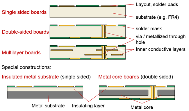
Classification of Printed Wiring Boards according to arrangement of the conductive planes:
Desgin criteria of conductor lines:
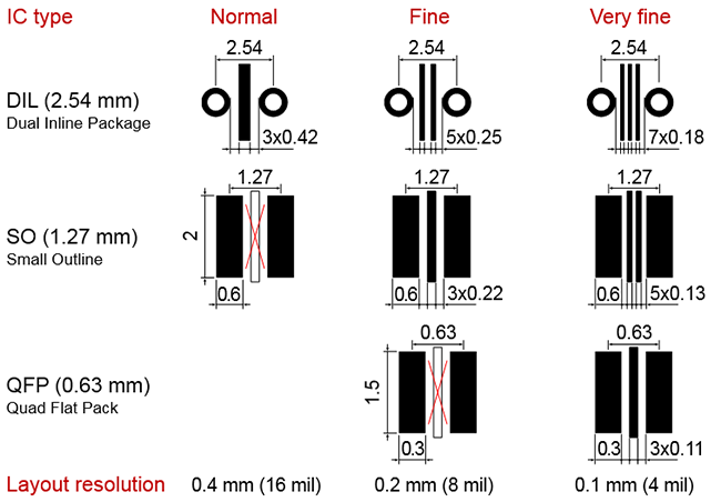
Layout definitions:
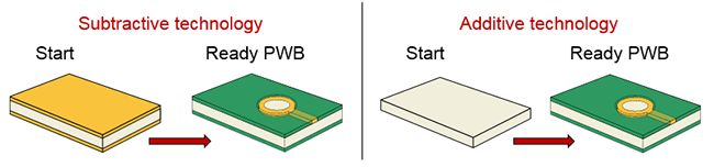
Subtractive technology: It starts with an insulating substrate covered with copper cladding on one or both sides, then the unnecessary copper surface (where no wiring is needed) is etched away. Good adhesion of the conductive layer. The resolution is limited because of under etching.
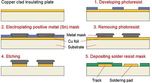
Additive technology (next lecture): The metal layer is deposited onto the insulating substrate only according to its layout (to those places which the mask did not cover). More complex layout, worse adhesion.
Semi-Additive technology (next lecture): Incorporate the advantages of above processes.
Basic technologies of PWB productions:
Mechanical technologies: cutting, drilling, brushing (deburring), milling.
Chemical technologies: cleaning (degreasing, microetching, oxide removing), coating (electrochemical, electroless), layer removal (etching), surface treatment, rinsing.
Masking technologies (pattern transfer): screenprinting, photoresist technology (photolitography)
Mechanical Technologies - Drilling:
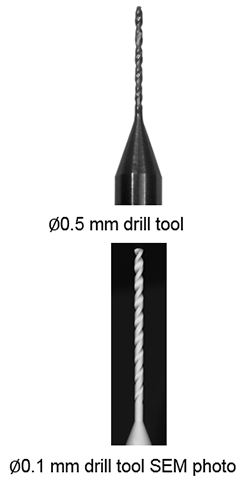
Technological parameters: main motion is the rotation of drill tool - circumferential (cut) speed (v, m/min); side motion is the movement perpendicular to the surface - feedrate (e, mm/rot.)
Material of drill tools: Requirement are the high quality simultaneous cutting of different substrate (materials: Cu, glass, epoxy...), the close tolerances and small surface roughness. Composition: 88...94 % tungsten carbide (WC) and 6...12 % cobalt (Co).
Layer depostion techniques:
Electroplating – only onto conductive surfaces, on equipotential surface
Electroless („chemical”) coating – on catalyst insulating plate
„Direct” plating – conductive compound is deposited onto surface of holes, thus improving conductivity (~kΩ) thus, electroplating becomes possible
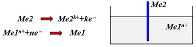
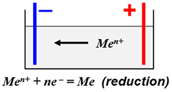
Immersion process – driven by standard potential difference between metals („ion exchange”)
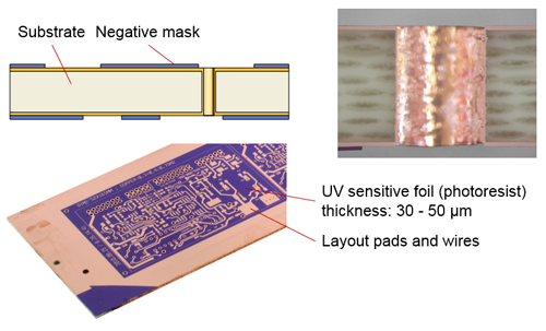
Masking techniques - Photoresist technology
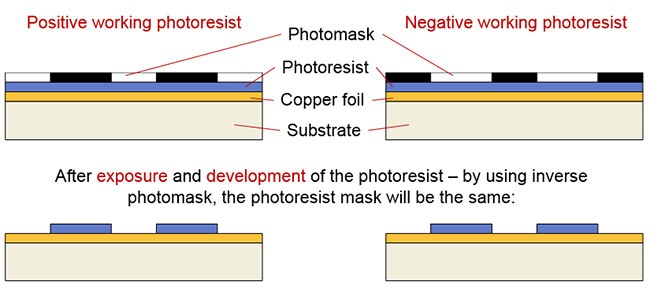
Positive working photoresists: exposed parts become soluble.
Negative working photoresists : exposed parts become insoluble
Negative working photoresists : exposed parts become insoluble
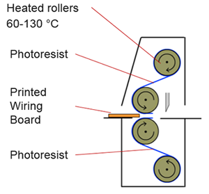
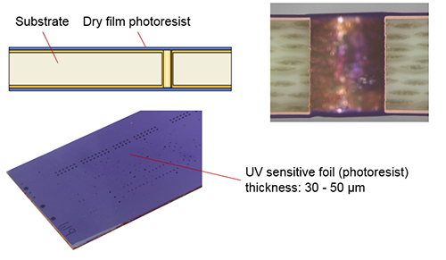
Dry film photoresist coating:
Technology of one-side PWBs
Technological steps when using positive photoresist mask:
Technological steps when using negative photoresist mask:
Technology of double-side PWBs
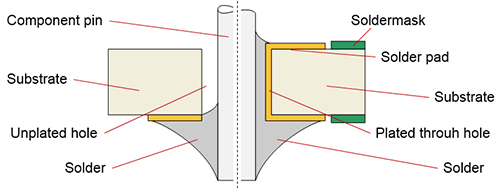
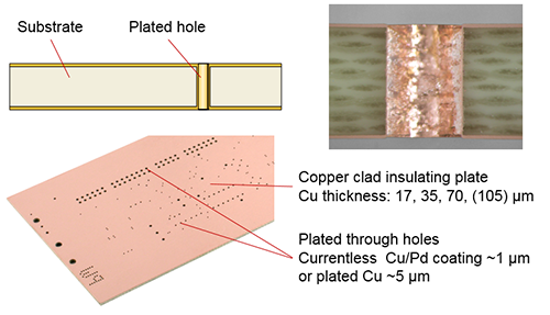
The aim of the through-hole metallization: electrical connection among conductive planes and reliable solder joints when using through hole components.
Making of through hole plating: copper deposition by electroless process – resistance of through hole ~mΩ; chemical deposition of conductive compound – resistance of hole surface ~kΩ; then electroplating of copper on equipotential surface.
Making of through hole plating: copper deposition by electroless process – resistance of through hole ~mΩ; chemical deposition of conductive compound – resistance of hole surface ~kΩ; then electroplating of copper on equipotential surface.
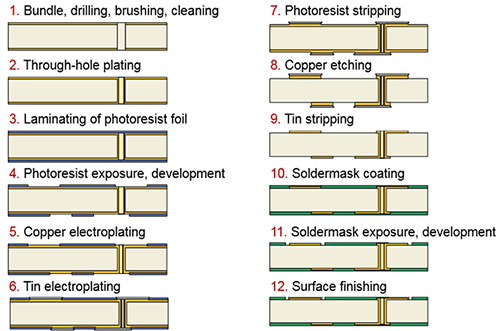
Production steps:
- Starting (subtractive technology): copper clad insulating plate
- Bundle making, drilling, brushing, cleanin
- Through-hole plating (a: currentless layer + electroplating, b: direct plating)
- Laminating dry film photoresist
- Photoresist exposure, development, drying, dissolution, cleaning
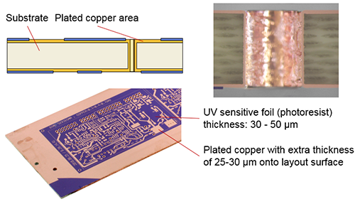
- Copper electroplating– increasing hole and layout metal thickness
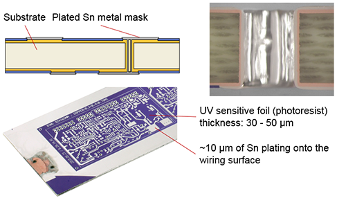
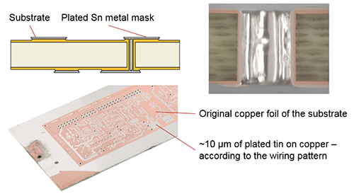
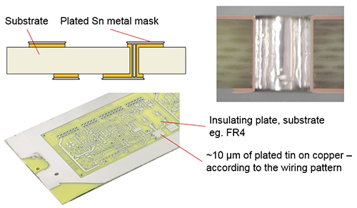
- Tin (Sn) plating – metal mask against copper etching
- Photoresist stripping
- Etching of copper
- Tin stripping
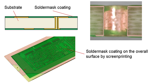
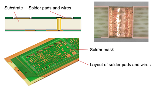
- Photosensitive soldermask – applying e.g. by screenprinting
- Solder mask – exposure through photomask, then development
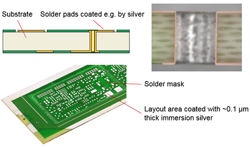
- Protecting solder pads from oxidation, e.g. immersion silver
Production steps: of double sided PWB (Summary)
Surface finnishes of PWBs:
- Hot Air Solder Leveling(HASL): immersion to solder bath and hot air smoothing
- Immersion tin (ImSn), the process: Sn2++2Cu -> Sn+2Cu+
- Immersion silver (ImAg),the process: 2Ag++Cu -> 2Ag+Cu2+
- Organic Solderability Preservative (OSP)
- Electroless Nickel / Immersion Gold (ENIG)
Finishes used earlier, like electroplated tin or tin-lead, are not suitable anymore because of „orange effect” (solder mask cracking) and environmental considerations.
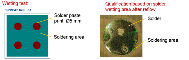
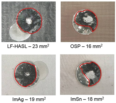
Wettability of surface finishes after 1 thermal cycle
The lead-free hot air soldered leveled (LF-HASL) coating has the best wettability, but it cannot be applied for fine-pitch QFP/BGA components due to its rough surface. ImSn/ImAg coatings are smooth and even; their price and wettability is medium. The OSP coating has the worst wettability but due to its low price, it is applied in low-cost consumer electronics.
| Previous | Next |