
2- Electronic assembly technologies
2.1 - Wave soldering technology
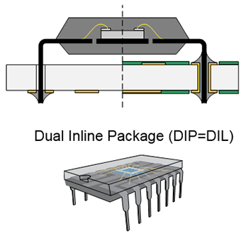
Through Hole Technology
The component leads are inserted through the holes of the printed wiring board (PWB); and soldered to the lands on its other side. Disadvantages of Through-Hole mount: uses both sides of the PCB, the area occupied by a component is large, because of the thick leads and large holes, when the I/O lead number is high (>40), the automated insertion is very difficult, package shapes are not standardized, pitch of the leads is inaccurate. After component placement, the joining method is hand- or wave soldering.
Soldering is a process in which two or more metal items are joined together by melting and flowing a filler metal into the joint; the filler metal has lower melting point than the workpieces. The solder is molten, it wets the surfaces, and the (adhesion-diffusion type) joint is formed when the solder is cooled down and re-solidifies.
Lead-free solder paste alloys:
| 96.5Sn3Ag0.5Cu | Tin-Silver-Copper | melting temp. 217°C |
|---|---|---|
| 96.5Sn3.5Ag | Tin-Silver | melting temp. 221°C |
| 99.3Sn0.7Cu | Tin-Copper paste | melting temp. 227°C |
The role of fluxes are to clean the surfaces and remove oxides and to enhance wetting properties of the solder.
Solvent: alcohol, water.
Solid phase: rosin, resin.
Activator: halogen-bearing, halogen-free.
No-clean flux: cleaning the board from flux residues after soldering is not necessary.
VOC-free: does not contain Volatile Organic Compounds.
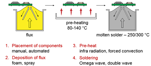
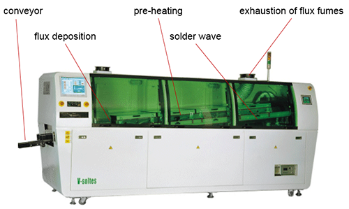
Steps of wave soldering
Wave soldering is the most popular automated soldering method for through-hole components. Both the heat and the solder are provided by the solder wave. The board is moved through the soldering system by a conveyor with a speed of ca 1,3-1,5 m/min.
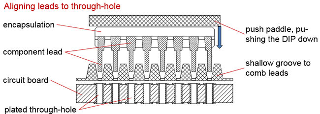
Automated insertion of thrugh-hole components
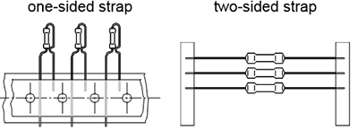
- Cutting out the component from the strap, in which it is placed in the proper order
- Picking the component up, bending its leads for the right shape, then positioning both the component and the bending unit
- Inserting the component into the holes of the board, cutting the leads of the component
- Fixing the components by bending its leads
Inertion of thrugh-hole active components (DIP insertion):
From the plastick tubes, the components are inserted with placement heads, called DIP tools inserted DIP component
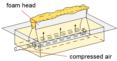
Flux depostion
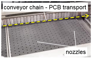
Foam fluxing: foam fluxing is simple and cheap, but the foam forming depends on the distribution of the blown compressed air, along the 50–60 cm long foam head the intensity of the foam formation varies.
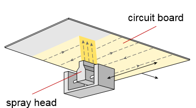
Spray fluxing: the flux is vaporized through nozzles and sprayed to the PCB, the amount and the distribution of the deposited flux can be controlled more precisely, the technology is sensitive to the variation of the flux density.
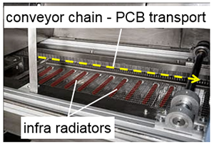
Pre-heating
The role of pre-heating is to activate the flux to remove oxides from the pads and to heat the circuit before wave soldering; thus, eliminating/lowering the thermal shock of the printed circuit board during dwell. The typical end temperature of pre-heating is 80–140°C.
Infra radiation type: advantage is the good efficiency but the components made from different materials may heat up differently.
Forced convection: advantage is the uniform heat transport but disadvantage is the lower efficiency.
Types of wave soldering
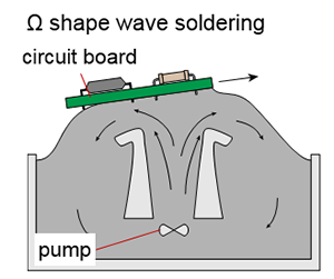
One wave (Omega wave) soldering:
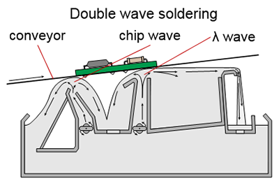
Double wave soldering:
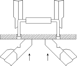
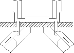
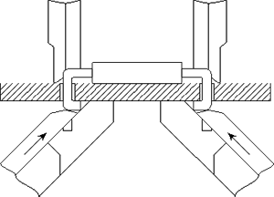
Chip wave: turbulent, fast flow velocity wave, provides the necessary amount of solder to the soldering pads.
λ wave: laminar, slow flow velocity wave, removes excessive solder and eliminates solder bridges.
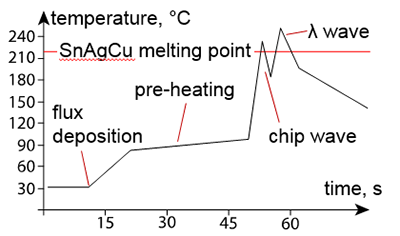
Thermal profile of the wave soldering:
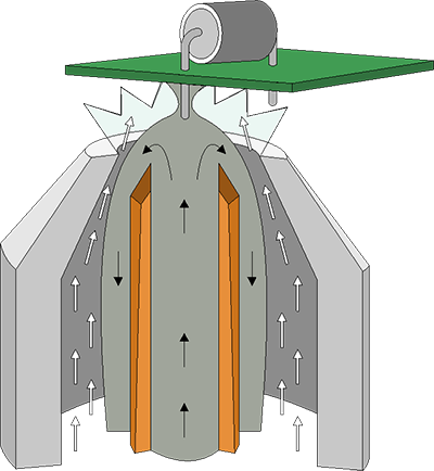
The wave soldering machine:
Wave soldering of surface mounted components
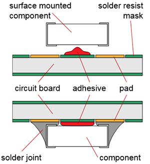
The surface mounted components can be soldered by wave soldering too, but they have to be glued onto the printed circuit board. Steps before wave soldering for surface mounted components:
- Depositing adhesives onto the circuit board according to component locations
- Placing components into the adhesive
- Curing adhesive at around 150 °C; after curing the component is mechanically fixed
- Turning the printed circuit board upside down and doing wave soldering (flux deposition, pre-heating, soldering)
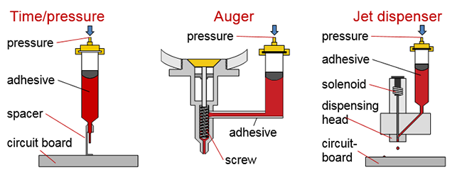
Dispensing of adhesives:
Time/pressure, auger: the contact methods, spacer might harm the circuit board; the amount of deposited adhesive depends on the diameter of the dispensing needle, on the length of the spacer as well as the viscosity of the adhesive.
Jet dispenser: a non-contact method; fast and accurate (~20.000 dots/hour); the relative deviation of dot volume is around 5-10%; the cleaning of the tool is difficult.
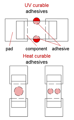
Curing of adhesives:
The necessary time and temperature to cure adhesives: approximately 10–15 minutes and above 100–110 °C, this can slightly vary from adhesive types and manufacturers. Adhesives are not sensitive to overheating and to fast heat-up or cool-down, generally, at higher temperatures, adhesives polymerize faster.
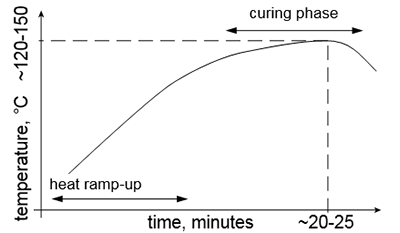
Thermal profile of the adhesive curing:
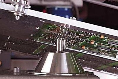
Mini-wave soldering:
Typically uses a miniature pumped solder wave with a spherical shape to solder the PCBs’ joints one by one. This process is somewhat slower than the previous methods, but much more accurate. The PCB may be fixed and the wave solder pot is moved underneath the PCB in 3-axis, or alternately the PCB may be positioned over a fixed wave/solder bath to perform the selective soldering process.
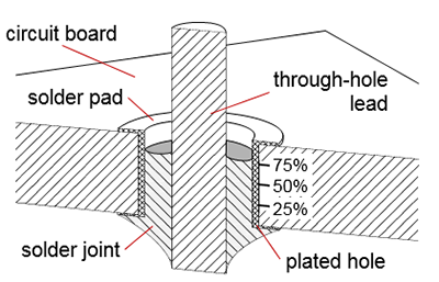
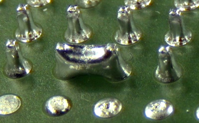
Quality requirements of through-hole solder joints:
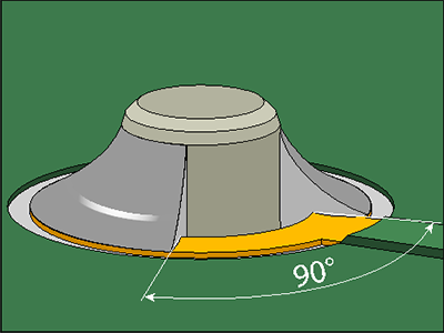
A good quality solder joint is shiny (lead-free is slightly dull), clean, smooth, and has a homogeneous surface; its cross-section is concave. Wetting around the pin is 270/330°, percentage of land area covered >75%, vertical fill of solder 75%, the 25% unfilled height includes both source and destination side depressions.
Soldering deffects of wave soldering:
- temperature of the solder is too low
- inappropriate pre-heating
- inadequate flux activation
- conveyor speed is too high
- the pad on the circuit board or the lead is poorly solderable
- solder wave height is too low, or inhomogeneous
- inadequate flux activation
- small amount of deposited flux
- conveyor speed too high
- shadowing effect of other components
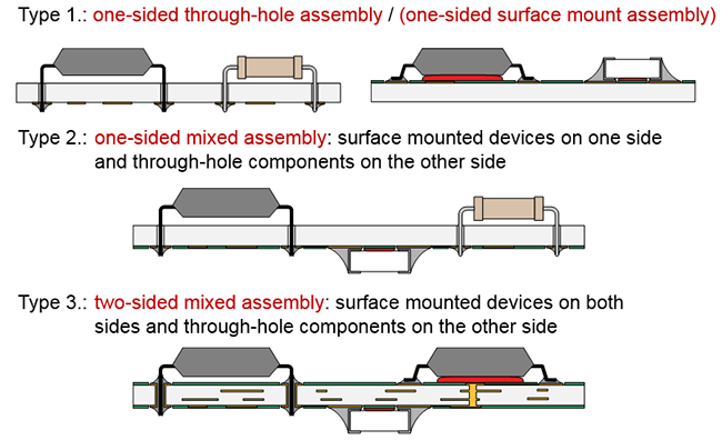
Assembling types of electronics circuits prepared by wave soldering:
| Previous | Next |