
6 - Technology of printed wiring boards
6.2. Manufacturing technologies of multi-layer printed wiring boards (PWBs)
Layout definition
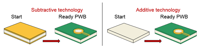
Subtractive technology:It starts with an insulating substrate covered with copper cladding on one or both sides, then the unnecessary copper surface (where no wiring is needed) is etched away. Good adhesion of the conductive layer. The resolution is limited because of under etching.
Additive technology: The metal layer is deposited onto the insulating substrate only according to its layout (to those places which the mask did not cover). More complex layout, worse adhesion.

Semi-Additive technology: Incorporate the advantages of above processes
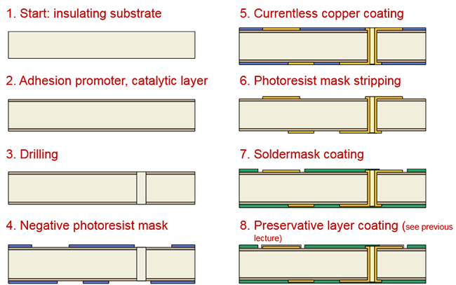
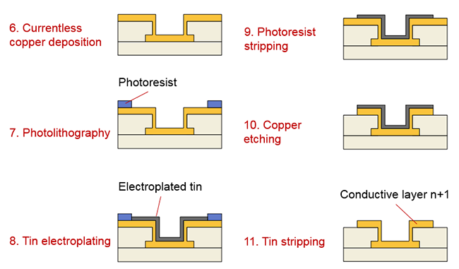
Additive technology of PWBs:
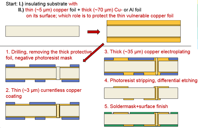
Semi-additive technology of PWBs:
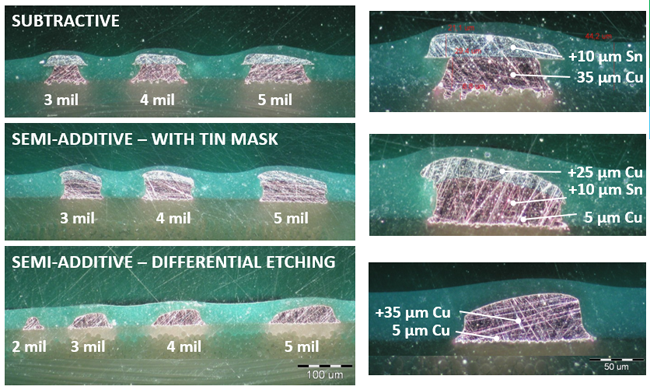
Comparing layout definition technologies:
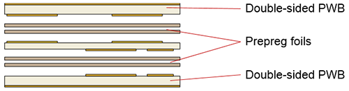
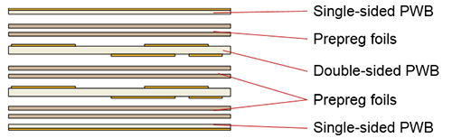
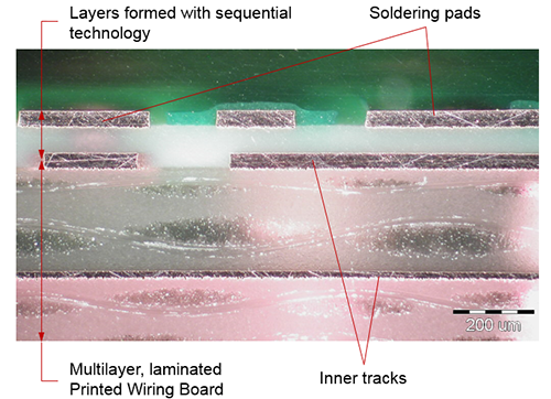
Co-laminated multilayer PWBs
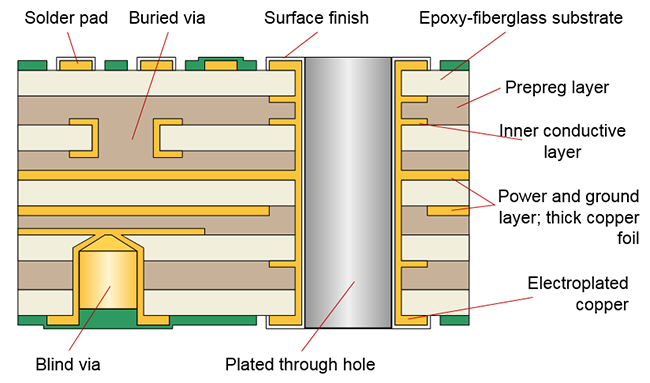
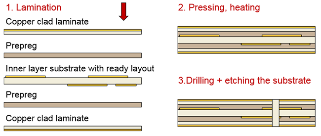
The number of layers of multilayer printed wiring boards are determined by the number of conductive layers. The process starts from single- or double-sided printed wiring boards. Each inner layer must have its wiring and surface of copper must be ready for pressing (oxidation to get CuO and Cu2O). The buried vias are already on the substrates in this stage. Co-laminating technology: substrates are sticked by (pre-impregnated) prepreg epoxy foils. Hardening of prepegs being between precisely aligned substrate takes 30…60 minutes at temperature 170 °C, applying a pressure of 150 N/cm2. After co-lamination the technology of external layout formation corresponds to the double-sided printed wiring board technology. (see: previous lecture).
Layers and holes in multilayer PWBs:
Technology of multilayer PWBs:
The technology of the external layout formation from this stage corresponds to the double-sided printed wiring board technology(see: previous lecture)
Bulid-up variations of multilayer PWBs:
Cheaper, low accuracy; misalignment of the layers can be caused by both the photomask and substrate positioning inaccuracy.
More expensive, higher accuracy; misalignment of layers is only caused by photomask positioning inaccuracy.
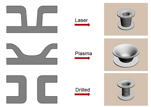
Microvia forming technologies:
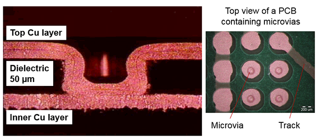
Microvias are plated through-holes connecting conductive layers of the wiring with diameter of 10...100 µm. Advantages of usings microvias: shorter wires - higher speed of signals – faster operation; smaller dimensions because of smaller hole diameter and soldering pad size; less parasitic effects, less noise; higher reliability.
Technologies for Microvia production: hole preparation into copper clad laminates, then hole metallization. For large diameters, mechanical drilling is economical, for small diameters, laser drilling, plasmaetching, or photolithography is used. Through-hole metallization: onto the surface of holes, or via filling.
Different microvia structures:
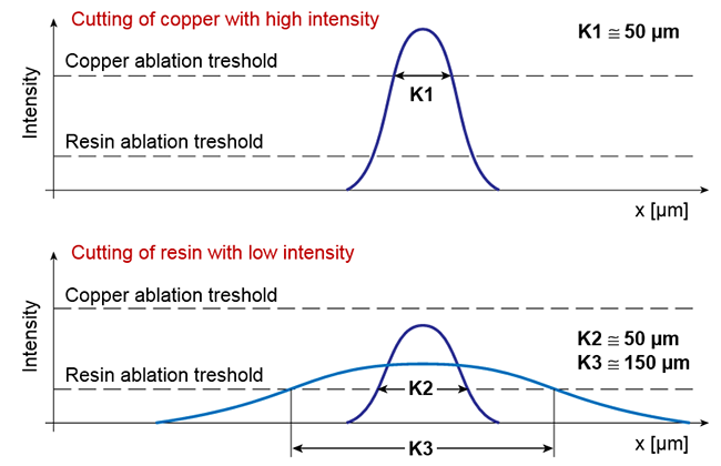
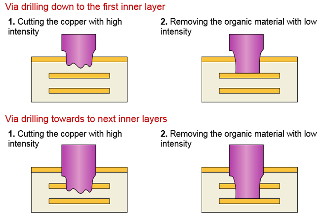
UV laser drilling:
Steps of UV laser drilling:
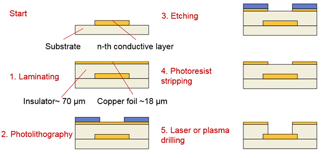
Sequential Build-Up (SBU) of multilayer PWBs:
Sequential technology: in multilayer PWB is built up by depositing insulating and conductive layers one after the other. Connections among the conductive layers are made by microvias.
Layer formation in SBU multilayer PWBs
High density, microvia PWBs: 10…100 µm vias are generated in the layers of multilayer PWBs, that are formed sequentially on top of each other – one conducting, one dielectric layer.
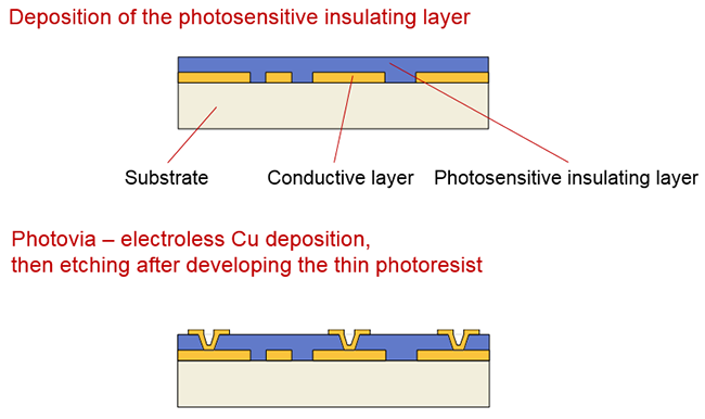
SBU technologies using photosensitive insulating layers:
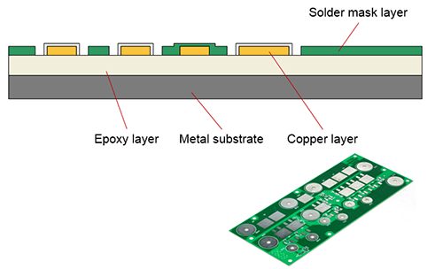
Special (IMS) Insulated Metal Substrate PWBs
Insulated Metal Substrate (IMS): Al metal plate coated with insulating layer then laminated with copper foil. Purpose of application is the improving heat conductivity. Epoxy-fiberglass substrate has 0.2 W/(mK) while IMS substrate has 1.3 W/(mK).
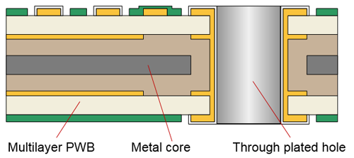
Special metal core PWBs
Purpose: matching the thermal expansion coefficient of the substrate to that of the components to be soldered (e.g. ceramic based components. Thermal expansion coefficient of epoxy-fiberglass is 12…16 ppm/°C, while CCC package has 5,9…7,4 ppm/°C. Metal core plates (~ 5 ppm/°C), (Cu-Mo-Cu (CMC) and Cu-Invar-Cu (CIC)).
Mulit Chip Modules (MCM)
By their name, multichip modules are assembled circuit modules containing several chips. More exactly, most important properties of MCMs: Contains at least 2 unpacked chips, substrates are High Density Interconnections (HDI), and have effective cooling system. MCMs are classified according to the processing technology of the substrate production:
- MCM-L – MCM-laminated: the substrate of the laminated type multichip modules is a multilayer PWB
- MCM-D – MCM-deposited: modules assembled on substrates made by thin film vacuum (deposition) technology
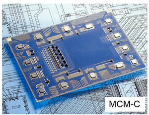
- MCM-C – MCM-ceramic: multilayer ceramic substrate modules
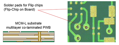
MCM-L substrate: HDI PWB
MCM-L: laminated multichip module. The substrate is a high density multilayer PWB with microvias and a complex layout circuitry. It can be made by lamination, sequential build up, or with combination of these. Multilayer PWBs are made by adhering single- or double-sided boards, or by sequential layer build up. Layout pattern is made by a combination of photolithography, plating and etching. Layers above each other are connected by plating through-holes or by microvias.
MCM-D substrate: Made by thin film technology
In the case of MCM-D multichip modules, the dielectric layer is polymer, or SiO2 (used in semiconductor technology), or other insulating film in a multilayer structure. Metallization is made by vacuum technology used in thin film processing. Conductive layout pattern is made by photolithography.
Materials of the substrate: ceramic (Al2O3 ; BeO; AlN), glass (e.g. borosilicate), silicon, diamond.
Dielectric materials: polyimide, parilene, poly-benzo-ciklobuthane (BCB), silicon-dioxide (in case of silicon substrate).
Silicone MCM-D substrate: Made by thin film technology
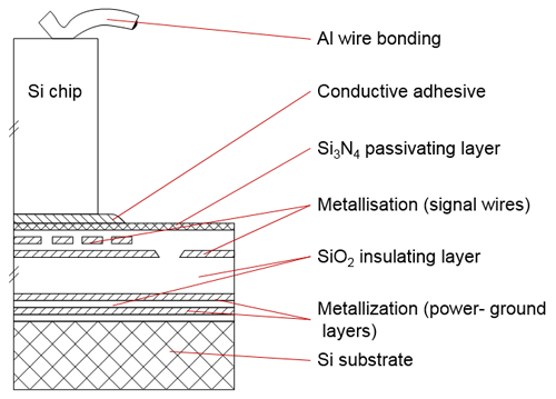
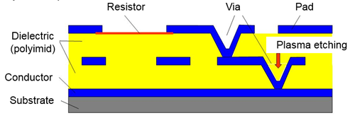
Sequential bulid up MCM-D substrate
The first conductive layer is made on the surface of the substrate by thin film technology. Then a dielectric layer is deposited onto this layer from liquid form, by spin-coating or printing. Small apertures (microvias) are opened into the dielectric layer. Then the total surface is covered by metallization. The layout pattern is made from the upper metal layer by photolithography and etching. The above steps are repeated several times from the deposition of the dielectric layer. In this way, multilayer substrates with 8-10 conductive layers are produced.
MCM-C multilayer ceramic substrate modules
Types of MCM-C multichip modules (see topic 4.1 and 4.2):
- TFC (Thick-Film Circuits): Thick-film hybrid ICs are formed by screen printing on ceramic substrate.
- HTCC (High Temperature Cofired Ceramic): multilayer ceramic substrates fired on temperatures higher than 1500 °C.
- LTCC (Low Temperature Cofired Ceramic): multilayer ceramic substrates fired on relatively low temperature (800…1000 °C).
| Previous | Next |