
5 - Thick-film technology
5.1 - Ceramic and polymer thick-films
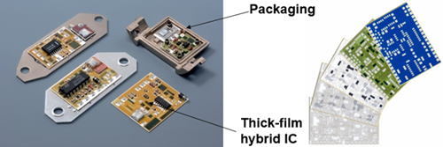
Insulating substrate integrated circuits and thick-film technology
In insulating substrate IC-s, the conductor pattern connecting the Valami link!!! components, the majority of resistors and other passive components are realized in integrated form by thick- or thin-film technology on the surface of the substrate. We distinguish two different types according to the production technology: thick-film and thin-film IC-s. If further components (so-called hybrid elements) are also mounted onto the substrate as discrete components, then we call the circuit a hybrid IC.
Thick-film: a typically 5-50 µm thick layer prepared from a paste by screen printing and heat annealing technology, usually onto ceramic (sometimes glass, silicon, insulated metal) or plastic substrates.
Materials
Thick-film pastes: colloid suspension materials consisting of
- functional phase (which determines the behavior of the final film),
- inorganic and/or organic binder materials,
- solvents.
- inorganic (glass/frit or chemically) bonded pastes,
- organic (polymer) bonded pastes.
Basic materials ceramic (pastes) consist of:
Functional phase:
Functional phase:
- For conducting layers: Ag-Pd, Au, Cu, W
- For resistive layers: oxides of Ruthenium, Iridium and Rhenium (RuO2)
- Low melting point glass (SiO2)
- Lowering the melting point with B, Ba, Pb
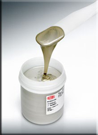
Polymer Paste composition:
Functional phase:
Functional phase:
- Conductor paste: Ag, Cu
- Resistor paste: C
- thermo-plastic pastes: (the paste hardens when the solvents dry off; if heated, the film will soften reversibly),
- thermo-set pastes (during curing, the polymer is irreversibly cross-linked making a stable matrix resistant to solvent and reheating),
- UV curable pastes: cross-linking is generated by UV light.
Thick film integrated components:
The realizable integrated components in thick film circuits are passives: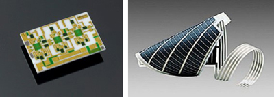 The layers are prepared by repeated subsequent printing of various thick film pastes. The integrated form of the capacitors and inductivities is rarely used because of the big space demand and the large production value tolerance. Instead, discrete hybrid components are applied. The discrete components can be mounted onto the contact pads by soldering or gluing. Unpackaged chips can be also placed to the surface of the thick film circuit which are usually connected to the circuit by wire bonding, and then the chips are secured from the environment impacts by „globe-top” packaging technology (i.e. protective layer dispensing). The value of the integrated resistive components can be corrected by laser value-calibration method, called laser trimming of the resistors.
The realizable integrated components in thick film circuits are passives:
- conductive wiring,
- crossovers and multi-layer structures,
- contact pads (for I/O pins and for the discrete hybrid components),
- resistor (constant value; temperature dependent ,voltage dependent types),
- capacitors,
- inductivities.
The layers are prepared by repeated subsequent printing of various thick film pastes. The integrated form of the capacitors and inductivities is rarely used because of the big space demand and the large production value tolerance. Instead, discrete hybrid components are applied. The discrete components can be mounted onto the contact pads by soldering or gluing. Unpackaged chips can be also placed to the surface of the thick film circuit which are usually connected to the circuit by wire bonding, and then the chips are secured from the environment impacts by „globe-top” packaging technology (i.e. protective layer dispensing). The value of the integrated resistive components can be corrected by laser value-calibration method, called laser trimming of the resistors.
Thick-film substrates:
Thick-film substrates: thick film circuits are produced on pre-manufactured substrates: Ceramics (for organic and inorganic pastes):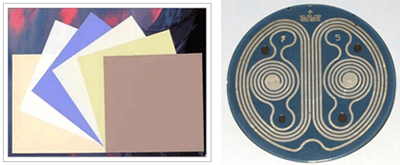
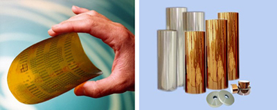 The main advantages of the widely used ceramic substrates: good thermal stability, low thermal expansion and small permittivity, which make the ceramic substrates favorable for high power, high frequency and precision applications. The cheap flexible polymers are very good for less sophisticated applications (e.g. keyboards, toys, consumer applications). Besides, thanks to the flexibility, they are also good for connection between moving components or 3D cambered unites (e.g. circuit of the digital cameras).
Thick-film substrates: thick film circuits are produced on pre-manufactured substrates: Ceramics (for organic and inorganic pastes):
- alumina (Al2O3)
- beryllia (BeO)
- aluminium-nitride (AlN)
- epoxy based flexible or rigid (FR4) substrates
- polyimide foil
- polyester foil
The main advantages of the widely used ceramic substrates: good thermal stability, low thermal expansion and small permittivity, which make the ceramic substrates favorable for high power, high frequency and precision applications. The cheap flexible polymers are very good for less sophisticated applications (e.g. keyboards, toys, consumer applications). Besides, thanks to the flexibility, they are also good for connection between moving components or 3D cambered unites (e.g. circuit of the digital cameras).
Manufacturing Technology:
1. Screen printing technology: screen printing is the most widespread and common additive layer deposition and patterning method in thick film technology. Paste printing is carried out by a screen printer machine. The screen is strained into an aluminium frame and the thick film paste is pressed onto the carrier through it by a printing squeegee. The squeegee has constant speed and pushes the screen with contact force. The material of the screen can be stainless steel or polymer. The design of the printed layer is realized with a negative emulsion mask on polymer screens while with openings on stainless steel metal masks. The main process steps of screen printing are the following:
- Insertion of the screen into the printer
- Placement of the thick film paste on the screen
- Insertion of the substrate into the screen printer
- Positioning
- Paste printing
- Separation (snap-off) of the screen from the substrate
2. Heat annealing processes in thick-film technologies: technologies of both polymer and inorganic thick films are presented together here due to their similarities. After all technology steps references are marked accordingly (polymer – P, inorganic – I).
Thermal profile for inorganic pastes: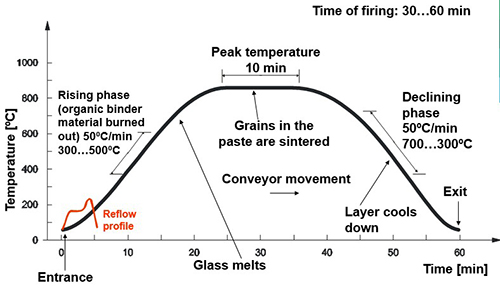
- Levelling of the deposited paste: at room temperature, 5 - 10 minutes (P,I): Screen printed thick-film pastes need some time for the acceptable levelling of the surface, to smooth out the imprint of the screen meshes.
- Drying: (P,I): The process is performed in a convection drying case or in an infrared oven. It takes 10 - 15 minutes. The temperature during drying is between 120 – 150 °C. The aim of this process is to remove the solvent components from the printed paste.
- Firing (burning) of the thick film paste: Inorganic:
- thermo-plastic pastes: (the paste hardens when the solvents dry off; if heated, the film will soften reversibly) on polyester need only a drying process at 120 °C for 15 minutes (widespread)
- thermo-set pastes (during curing, the polymer is irreversibly cross-linked making a stable matrix resistant to solvent and reheating) on polyimide substrates: after drying, burning is performed at 180 - 350 °C for 100- 180 minutes
- UV curable pastes: after UV illumination, a burning is made at 120 – 150 °C for 15 – 60 minutes
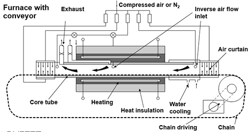
It is made at 750 – 950 °C in the case of inorganic pastes, the cycle time is 40 - 60 minutes in multi-zone conveyor furnaces.
Plastic:
Firing furnance:
Thermal profile for inorganic pastes:
The screen mask
Mesh number: number of apertures / 1 inch.
Mesh numbers applied in thick film technology: 80…350.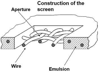 The Mesh number determines the thickness of the printed layer! Each layer needs different screen mask.
Mesh numbers applied in thick film technology: 80…350.
- conductor layer: 200…325
- resistor layer: 160…250
- solder paste: 80…90
The Mesh number determines the thickness of the printed layer! Each layer needs different screen mask.
Types of screen masks
Direct emulsion mask: application of a photo-sensitive emulsion layer and its photolithographic patterning directly on the screen. (Durable, but the thickness is not homogeneous.)
Indirect emulsion mask: the photolithographic patterning of a solid photo-sensitive foil, that is then rolled onto the mesh. (Thickness is homogeneous but the screen is easily damaged.)
Combined emulsion mask: Combines the advantages of the previous two types, but is expensive. (Suitable for printing thick layers due to the thicker emulsion layer on the mesh.)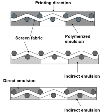
Production of hybrid IC
Animáció!
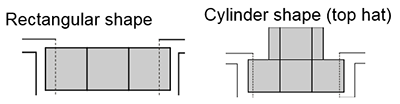
Shapes and trimming tracks of integrated resistors
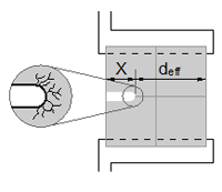
During trimming, usually an insulating cut is produced into the layer by laser, in order to change the effective d and l values.
where is the specific resistance, is the layer thickness, is the length, is the width, and is the square resistance. Using this method, the resistance of the element can only be increased.
 The cutting shapes of thick film resistor trimming:
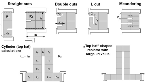
Shematic of the laser trimming: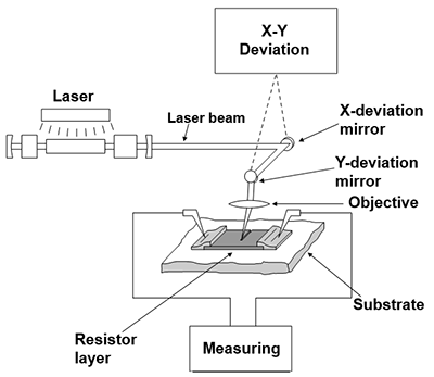
The cutting shapes of thick film resistor trimming:
Shematic of the laser trimming:
Ceramic thick film applications:
- Good heat conductivity: high current and power electronics
- Temperature resistance: high temperature applications
- Low dielectric constant: high frequency applications
- Resistor value correction is possible: special applications, active filters
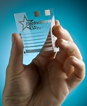
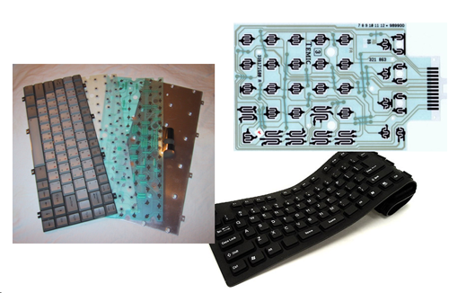
Polymer thick film applications:
Polymer thick film applications: polymer thick film technology is the most prevalent thick film technology thanks to its low price and simplicity, but its restricted reliability limits the application field of this technology in comparison with the inorganic thick films, see p. 1. The polymer thick film circuits are mainly used in the applications with low quality demand:
- passive part of custom electronics on FR4 substrate
- flexible interconnection-network for moving parts (printers, HD drivers)
- car electronics: mirror and seat heating foils
- specialties: smart labels
- keyboards and their accessories
Properties of thick-films
| Parameter | Ceramic thick-film | Polymer thick-film |
|---|---|---|
| TCR, ppm/°C | ±50 ... ±100 | ±200 ... ±500 |
| Deviation, R, % | ±20 ... ±30 | ±70 ... ±100 |
| Stability (1000 h) | <0.5% (150 °C) | <3 ...5% (80 °C) |
| Line resolution | 0.2 ... 0.1 mm | 0.5 ... 0.3 mm |
| Production cost | Moderate, expensive | Cheap |
| Previous | Next |