
1 - Technology of Electronics Products (TEP)
1.2- Classification of electronic products and technologies
Categories of electronics components and devices
Electronics components and devices can be categorized by:
- According to the function: active, passive
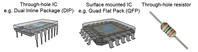
- According to the assembly: through-hole, surface mounted
- Number of functions: discrete components – one component contains one electronic device,
- Integrated circuits (IC) – one component contains many electronic devices
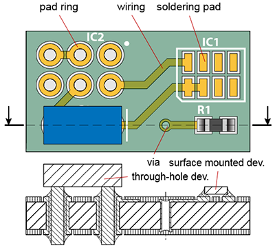
Build up of the printed wiring board:
- Substrate, e.g. FR4: glass-fiber epoxy
- Copper pattern: formed by photolitography
- Solder resist mask: deposited by screen printing, patterned by photolitography
- Text, silk screen: formed by screen printing
- Placing components: manual, automated
- Soldering: wave soldering, reflow soldering
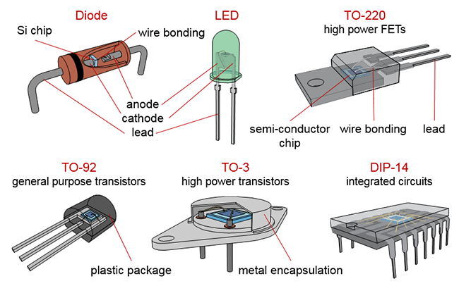
Through hole components
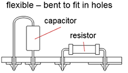
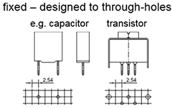
They have flexible or rigid/fixed leads. The flexible leads are bent according to the position of the holes in the Printed Wiring Board and cut to the proper size. At Through-Hole Technology (THT), component leads are inserted through the holes of the printed wiring board (PWB); and soldered to the lands on its other side. Thus, a TH assembly has a ′component side′ and a ′soldering side′.
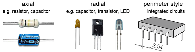
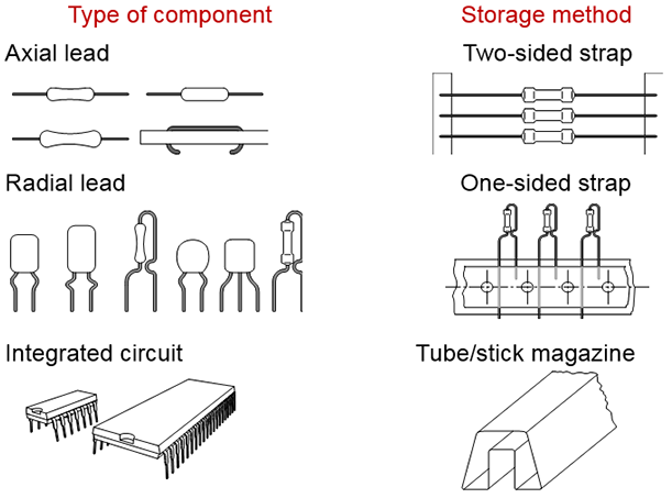
Classification of through hole components:
According to mechanical properties of the component leads:
According to geometry of leads:
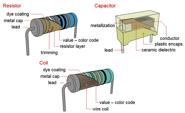
Discrete through hole components (Passives):
Discrete through hole components (Actives):
Special through hole components:
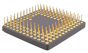
High lead-count through-hole components - PGA (Pin Grid Array). Leads are on the bottom of the package in a grid array; typical package type of Personal Computers CPUs. Advantage: can be placed into a socket with detachable mechanical joining changeable.
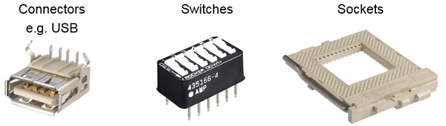
Electro-mechanical components:
Storage of the trough hole compoenents:
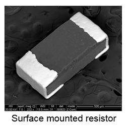
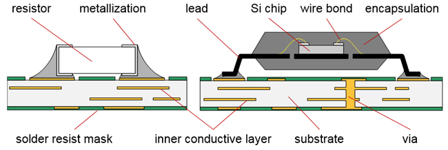
Surface mounted components
They have short leads (which are inappropriate for through-hole mounting) or solderable metallized terminals on the sides or on the bottom of the package. The copper pattern (footprint) on the Printed Wiring Board is designed according to the geometrical layout of the components’ terminals. The components are placed onto the soldering pads and they are soldered on the same side.
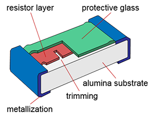
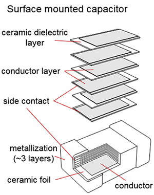
Discrete surface mounted components (Passives):
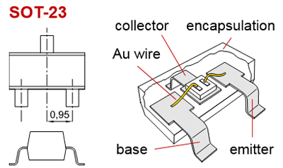
Discrete surface mounted components (Actives):
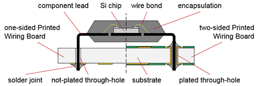
Role of package: protects the chip and provides compatibility between chip and PWB interconnects.
Level 1. interconnection: between the chip and carrier/substrate/interposer
Level 2. interconnection: between the chip carrier and printed wiring board
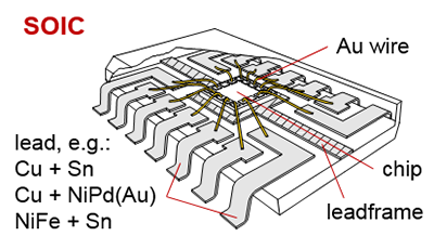
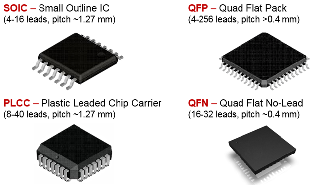
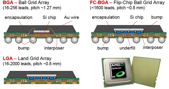
Classification of IC packages according to the lead geometry:
Packages with component leads in perimeter style:
Package with leads on the bottom of the package in area array style:
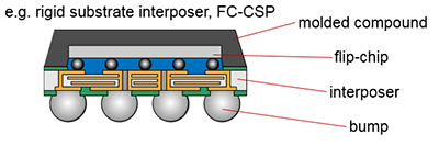
CSP - Chip Scale Packages:
According to IPC’s standard J-STD-012, package is qualified as chip scale, when the package has an area no greater than 1.2 times that of the die and it must be a single-die, direct surface mountable package. Classifications of the CSPs:
- flexible substrate interposer type
- rigid substrate interposer type
- leadframe type (perimeter style leads)
- wafer-level assembly type
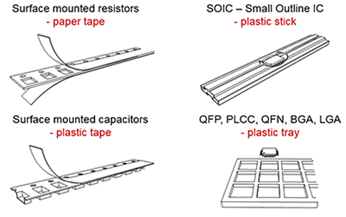
Storage of the surface mounted compoenents:
| Previous | Next |