4 - Technology of thin films
4.2 Film deposition and patterning technologies of thin film networks
Thin film:
We consider thin films those layers, that are deposited mostly on semiconductor, glass or flexible foil substrates and are typically prepared with same kind of vacuum technology, their thickness ranges from a few nm to a few um, often have different optical and/or conducting properties from the bulk material (their origin) from we can benefit.
Possible aplication of thin films:
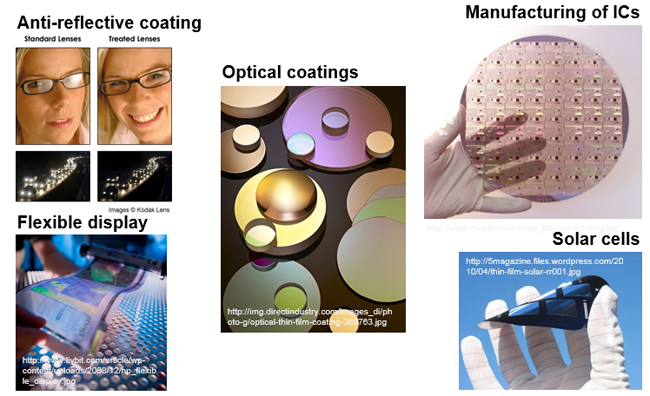
- optical (e.g. anti-reflection coatings, mirrors)
- electronic (e.g. interconnections on semiconductor circuits, thin film integrated circuits, solar cells)
- optical and electronic (e.g. transparent conductive films inside LCD displays)
- mechanical (e.g. wear-resistant coatings)
- surface passivation (e.g. preventing corrosion)
- self-cleaning surfaces (e.g. hydrophobic coating)
- decoration, arts
Thin film materials:
- Pure metal layers, e.g.: Gold (e.g. conductive layer); Aluminium (e.g. in CRTs, IC metallization, mirrors); Copper (e.g. wiring in thin film circuits)
- Alloys, compounds, e.g.: NiCr (nickel-chromium, a material of thin film resistors); TiN (titanium nitride, extra hard wear-resistant film); ITO (indium tin oxide, transparent conductive layers in LCDs); TaN (tantalum nitride, a special material of thin film resistors)
- Semiconducting layers: amorphous Si (thin film transistors in LCDs, solar cells); polycrystalline Si
- Dielectric layers, e.g.: MgF2 (optical anti-reflective layers)
Technology of vacuum evaporation and sputtering
Both technologies allow the deposition of thin-films of different materials, functions and thicknesses. They rely on vacuum, even though in case of sputtering gases (e.g. O2, Ar) of specific functions and amounts are filled into the vacuum chamber. Decomposition methods of materials into atoms or clusters to be deposited by evaporation with heating and by sputtering with ion bombardment.
The process of vacuum evaporation
Three important processes during layer deposition by vacuum evaporation:
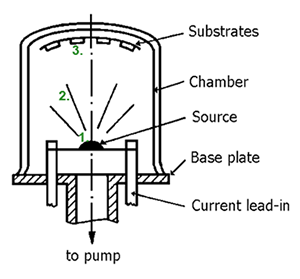
- Evaporation: decomposition of bulk material (source) into particles
- Material transport: particles migrate along a straight path according to the laws of radiation
- Condensation: particles condensate on the substrate, forming a layer
Evaporation sources - Direct and indirect heating by current
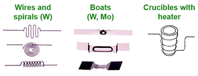
Goal: decomposition of bulk material into particles by heating
Evaporation sources - Electron beam evaporation
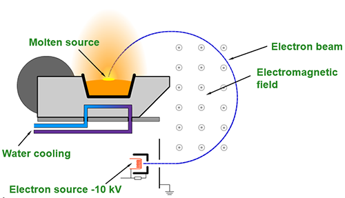
Heating is accomplished by colliding high-speed electrons with the bulk material. The kinetic energy of electrons transforms to heat. Why is the cathode hidden below the molten material: to avoid the evaporating atoms and their ions reaching the cathode this way.
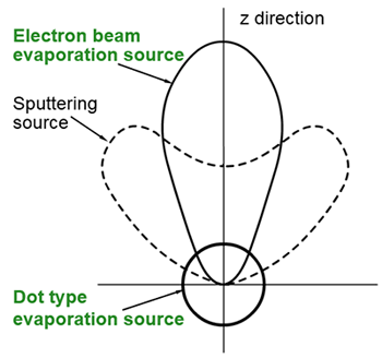
Radiation pattern of the evaporation sources:
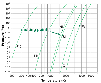
Evaporation rates as a function of temperature:
Relevance: All materials have different evaporation speed at a specific temperature. Important: Materials do evaporate even below their melting point.
The ion enhanced layer depostion: Surface of the substrate is bombarded by ions of specific energy during the layer deposition. Thus atoms are adsorbed on the surface, but those not yet fully attached to it are removed. Only atoms that have been bound to an island existing already on the surface remain there, as a result, denser and mechanically more stable layer is developed.
The process of vacuum sputtering
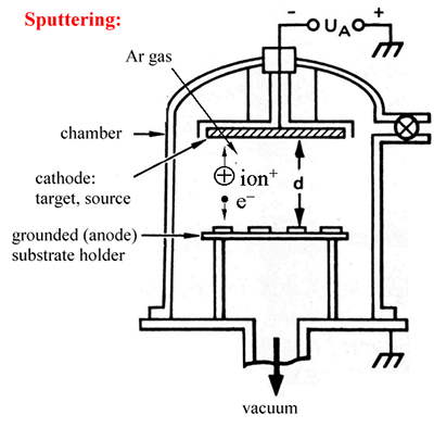
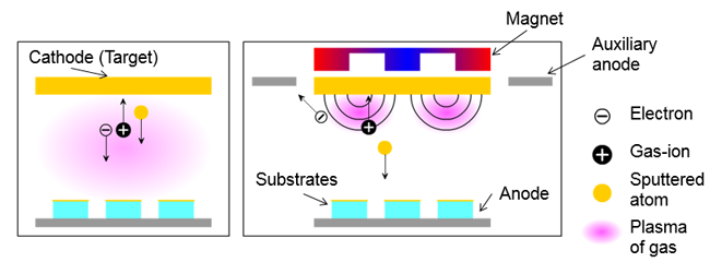
A way of bulk material (source) decomposition: not heating but bombarding with ions. Source called "target". Ions are generated by collisions of gas atoms and molecules with electrons.
Ionized positive gas ions accelerate towards the cathode (target) and eject (sputter) particles out of it, which will condense on the substrates placed on the anode. The acceleration of the negative electrons and positive ions are determined by the electromagnetic field generated between the source material (target) and the substrate holder (anode).
Implementation of vacuum sputtering - Magnetron sputtering: plasma is formed near the target with a magnet and auxiliary anode due to the more effective ion generation, the target is sputtered faster.
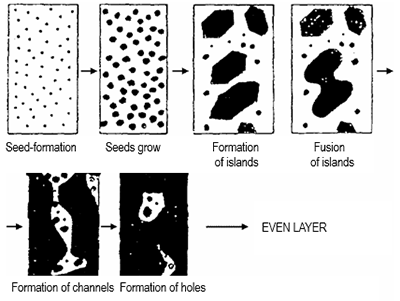
Evaulation of thin films on the surface:
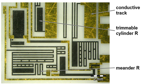
Thin film integrated circuits
Definition: circuits consisting of thin film resistors, capacitors, transistors and interconnections on insulating (mostly glass) substrates.
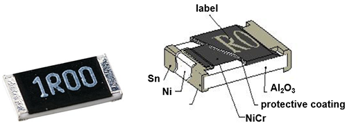
Wirings and contact pads: main requirements: good adhesion and conduction, compatibility with the joining techniques applied in electronics technology. Materials: Cu, Al and multilayer structures, e.g.: Cr-Au
Resistors: main requirements are the long-term stability and minimal thermal coefficient (TK or α, ΔR = α·ΔT·R). Materials: mostly alloys, or compounds e.g.: Ni-Cr (R□ = 100..200 Ω, α = ± 50 ppm/°C), Cr-Si, Ta2N.
Desgin of thin film circuits:
Sizing and production of thin film resistors: R = R□ · l/d, where R□ is the sheet resistivity of the material, l is the length, d is the width of the resistor. Hence the thickness of the layer is irrelevant during the design! R□ ~ 150 Ω in case of an 50-50% Ni-Cr resistor, but its production is not simple as the evaporation speeds of Ni and Cr are different at specific temperature and pressure values a simple resistor stripe will give a max. of a few 100 Ω, to gain higher resistances, meander form has to be designed. High precision value resistors are trimmed subsequently by a laser, providing precision better than ±0,1%. Important advantage: resistance values of resistors prepared with the same technology stay synchronized independent of temperature change (their ratio is constant).
Patterining methods of thin film circuits:
Patterning during layer deposition: deposition through a metal mask. Main advantage: the metal mask may not be in contact with the substrate. Main drawback: the technology is limited to a minimum of 500 µm line width.
Patterning after layer deposition has two types. Method one is the photolithography (as in Si and PWB technologies – see 2.5/5.1 topics). Main advantage: finer structures. Main drawback: the process is complicated, rather sensitive to cleanliness and technological parameters. Method two is the direct pattering by laser. Main advantage: flexible, the pattern can be changed anytime. Main drawback: lower productivity.
Tantalum (Ta) based thin film circuits
The interconnection, resistors and capacitors can be produced in one vacuum deposition cycle, hence changing the gas applied in the vacuum chamber enables the production of different components of the circuit. These processes are called reactive sputtering. Wiring: cathode sputtering Ta in Ar atmosphere; resistors: sputtering Ta in N2 atmosphere to Ta2N; and insulator: sputtering Ta in O2 atmosphere to Ta2O5 (dielectric for capacitors).
Example of prepearing of Ta based thin film circuits:
ANIMÁCIÓ!!
Specialities of photolitogrpahy in thin film technology - The LIFT-OFF technique
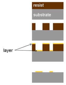
- resist (sacrificial layer) deposition
- exposition of the resist through a mask
- developing of the resist
- deposition of the layer material
- removing the remained photoresist which also removes the unwanted layer material
Important is that walls of the resist should not be covered by the layer material during the deposition process.