
3- Technology of semiconductor-based components
3.1. Mounting and encapsulation technologies of semiconductor devices
Mounting and packaging of semiconductor integrated circuits:
Chip mounting without packaging (chip on board, flip-chip on board):
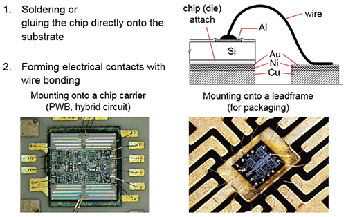
- Mounting by gluing or soldering
- Creating electric contacts (wire bonding, bump, or TAB)
- Protective coatings
Packaged integrated circuits:
- Materials for packaging (encapsulants)
- Methods for connecting ICs electrically : bonding wires and bumps
- Mounting of ICs inside packages: gluing, eutectic soldering
- Packaging technologies
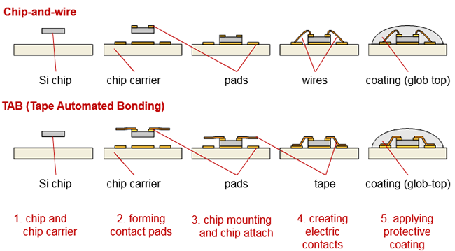
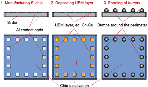
Chip mounting methods: Single chip + Wire bond; TAB
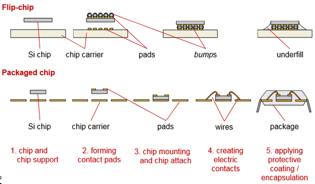
Chip mounting methods: Flip chip; Packaged chip
Chip whitout packages- (Flip-) chip on board
- Chip mounting and „die attach”: Onto the board (PWB, ceramic etc.), by gluing, or soldering, see: chip mounting techniques
- Creating electric contacts: Several options: Wire bonding, TAB, Flip-chip bonding (with bumps)
- Protective coating: „glob top” in the case of Chip-and-wire, underfill in the case of Flip-chip
Chip whitout packages- (Flip-) chip on board
- Chip mounting, „die attach”: By gluing and by soldering
- Establishing electric contacts: Wire bonding (Ultrasonic, Thermocompression, Thermosonic); TAB; Flip-chip bonding (with bumps)
- Packaging: (optional, without packaging: protective coating or underfill), „glob top” in the case of Chip-and-wire, underfill in the case of Flip-chip
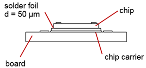
Chip mounting techniques: Soldering
Solder material availabilities:
preform foil - A pre-shaped foil (with thickness of 20-50 µm) is placed between the chip and the pad. This structure is fastened by a special clamp during soldering process.
coating (pre-plate) Solder materials are deposited on the chip and the pad.
paste Solder paste is stencil printed on the surface.
In the case of pre-form and pre-plate soldering, the atmosphere can be inert (pl.: N2), or reductive (pl. H2, ; formic acid - HCOOH). These gases provide oxide-free surfaces. In the case of the solder paste, this task is fulfilled by flux.
Solder material examples:
- 95Pb5Sn - mp. 314 ºC
- 80Au20Sn - mp. 280 ºC
- 80Au20Sn - mp. 280 ºC
- 95Sn, 5Sb – mp. 235-240 °C
- 65Sn, 25Ag, 10Sb – mp. 233 °C
- Thermal conductivity: ~ 60 W/mK
Soldering is used in the manufacturing of high-power electronics, where excellent thermal conductivity is required. Another advantage of soldering: after soldering, outgassing (from flux) does not occur. Because of the high temperature, soldering is not recommended for module circuits.
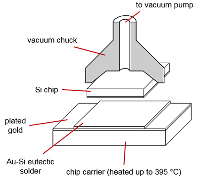
Chip mounting techniques: Eutectic Soldering
Process properties: N2 atmosphere, Plate heated slightly over the eutectic melting point, Chip is placed into the solder by a vacuum chuck
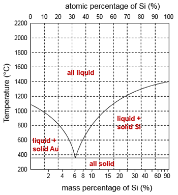
6m% Si, 94m% Au eutectic compound melts at 370 ºC.
Eutectics from Greek – easily melted) A mixture at a certain rate of two (or more) metal compounds, which has the lowest melting point possible.
Eutectics from Greek – easily melted) A mixture at a certain rate of two (or more) metal compounds, which has the lowest melting point possible.
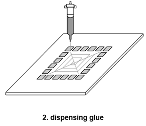
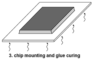
Chip mounting techniques: Gluing
Adhesives (glues) can be insulating or conductive. Conductive adhesives can be categorized according to the direction of conductivity:
- isotropic (conducts in all directions equally)
- anisotropic (conducts only in one direction)
Components of conductive adhesives: resin and filler resin:
Resin:
ANIMÁCIÓ!!!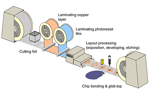
Resin:
- epoxy up to 175..250 ºC
- polyimide up to 400 ºC (polymerizes into 3D network)
- thermoplastics (up to 100 ºC)
- improving thermal conductivity: AlN, Al2O3, boron-nitride, diamond
- improving electrical conductivity : Ag, Au or Cu flakes
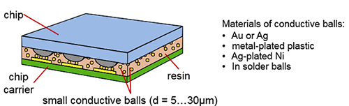
Chip mounting techniques: Anisotropic Adhesives
The conduction in the Z direction in ensured by some (10-15) conducting balls stuck between the contact pads facing each other. The contraction of the resin helps to create the contact. The anisotropic conducting adhesives are available also in solid film (d= 50 μm) and paste form.
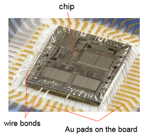
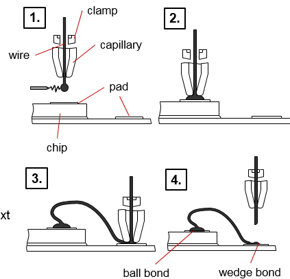
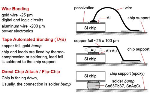
Wire Bonding:
Wire bonding Techniques: Thermocopression
- The end of the gold wire is heated up over the melting point by electric discharge.
- The gold ball is pressed vertically onto the pad.
- The wire is transported to the position of second bonding (e.g. pad on PWB, or on leadframe) .Clamp is closed; vertical pressure forms the second (wedge) bond.
- The capillary moves to the next bonding position.
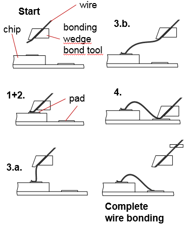
Wire bonding Techniques: Ultrasonic
- The wire fed through the bonding tool is pressed onto the bonding surface.
- Horizontal vibration is applied by ultrasound.
- Loop formation.
- Forming the second bond (same as step 2).
Clamp is closed, wire is broken by moving the tool away. The purpose of applying ultrasonic (US) vibration is to break the surface oxides and to approach suraces to atomic distance.
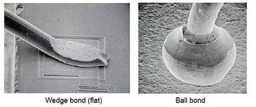
Wire bonding Techniques: Comparison
| Type | Method of bonding | Material of wire | Temperature | Shape of wire end | Bond force (typical) |
|---|---|---|---|---|---|
| Thermo-compression | Melting (softening), pressure | Au | 300-500 °C | ball/wedge | 15-25 mN |
| Ultrasonic | pressure,US vibration | Al, Au | 25 °C | wedge/wedge | 5-25 mN |
| Thermosonic | Elevated temp., pressure,US vibration | Au | 100-150 °C | ball/wedge | 5-25 mN |
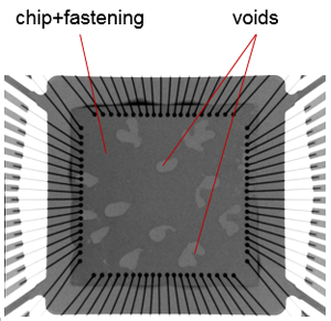
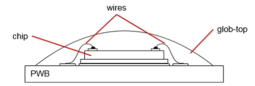
Protective Coating of Chip-on-Board Technolgy:
Glob Top (special resin-based coating) is dispensed over the chip bonding wires and then has to be cured (T=100 - 150°C). Purpose of glob top: mechanical, and chemical protection.
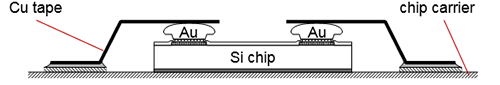
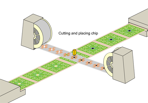
Tape Automated Boinding (TAB):
- Perforations are made at the edge of the tape, while windows for the chip are opened in the middle.
- A copper foil is laminated onto the plastic tape.
- A cantilever-like lead frame is formed from the Cu foil by photolithography and etching.
- Inserting and attaching the chip to foil leads. ILB (Inner Lead Bonding)
- Applying glob top coating.
- Cutting and bending of leads.
- Soldering onto the chip carrier
ANIMÁCIÓ!!!
TAB process:
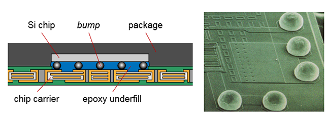
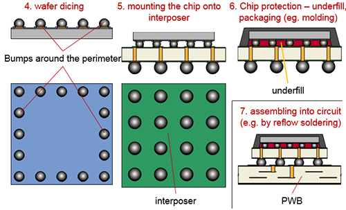
Flip-chip mounting technology:
The flip-chips (FCs) are (in conventional meaning) unpackaged Si chips equipped with small bumps over the conductor pads. These chips are placed face down to the substrate with their active side. The bumps are joint by soldering or gluing to the pads of the interconnection substrate. If the FC is mounted directly onto the PWB, it is called FCOB – Flip-Chip on Board)
Flip-chip mounting technology: Wafer-level techniques
Flip-chip mounting technology: Techniques with separate chips
Level 1 Interconnections:
| Previous | Next |