
3- Technology of semiconductor-based components
3.2. Silicon technologies
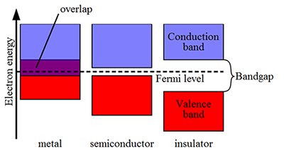
Band Structure
Electrical properties of metals and semiconductors are determined by their electron and crystal structure.
Simplified band structure shows the basic difference between metals, semiconductors and insulators.
Simplified band structure shows the basic difference between metals, semiconductors and insulators.
Semiconducting elements
Semiconducting elements – group IV (and their compounds) C, Si, Ge, α-Sn , or e.g. SiC
Dopants: Donors have more electrons (group V); Acceptors have less electrons (group III)
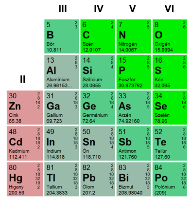
Compound semiconductors: pairs from group III-V and II-VI
Properties of semiconductors:
| Element | Band gap (eV) | Band gap (nm) | Type of band gap |
|---|---|---|---|
| Diamond (C) | 5,47 eV | 227 nm | Indirect |
| Silicon (Si) | 1,11 eV | 1127 nm | Indirect |
| Germanium (Ge) | 0,67 eV | 1851 nm | Indirect |
| Gallium-arsenide (GaAs) | 1,43 eV | 867 nm | Direct |
Crystal definitions:
Monocrystallic: The periodic repetition is perfect in a way that it covers the whole material (edge of the crytsal = failure)
Polycrystallic: (microcrystallic), the material is built up from many monocrystallic block
Amorphous: The long-distance periodic repetition of atoms is missing (there is only a short-distance order)
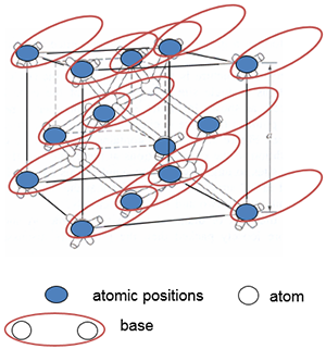
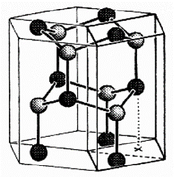
Crystal structure of the semiconductors:
Silicon (diamond structure): Two interpenetrated face-centered cubic (FCC) cells offset by l/4 cube diagonal. The „base” (atomic base) is made of two C atoms next to each other. The crystal structure is the offset of the atomic base by the all possible lattice vectors.
Unit cell: The smallest elementary unit of atoms possible in the structure of the crystal, repeated infinitely on a three dimensional lattice, defines the ultimate structure of the crystal.
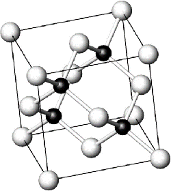
Crystal structure of the compound semiconductors:
Face-centered cubic lattice, the base consists two type of atoms (e.g. GaAs): Atomic positions are the same as in diamond lattice, but the atoms are altering.
Hexagonal lattice(e.g. GaN): The two types of atoms individually form hexagonal lattices.
Materials used in semiconductor technology:
| Material | Resistivity[Ωm] | Heat Conductivity [W/(mK)] | Density [g/cm3] | Form in semiconductor technology |
|---|---|---|---|---|
| Copper (Cu) | 16,7x10E-6 | 400 | 8,44 | polycrystallic |
| Silicon (Si) | 10E3 | 150 | 2,33 | single crystal(wafer), polycrystallic (electrode) |
| C (diamond) | 10E15-10E18 | 2000 | 352 | polycrystallic (CVD) |
| Silicon-dioxide (SiO2) | 10E16 | 1,38 | 2,63 | polycrystallic |
Properties of Silicone-dioxide:
SiO2, also known as silica, its crystallic form is quartz. Properties: electrical insulator (for gate dielectric), low thermal conductivity, high melting point (at 1830 °C (> Si)), and excellent chemical and mechanical stability (Hydrogen fluoride is the only acid that dissolves SiO2 (only etchant), therefore SiO2 is used for masking. Used for masking also during diffusion and implantation.)
Dielectric constant (k): „High-k” and „low-k” are common terms used in semiconductor manufacturing processes, it’s relative to the dielectric constant of SiO2 (k=3,9)
„high-k”: used as gate dielectric, it allows further miniaturization (numerator is increasing in the capacitance, so width(d) can be increased, too).
„low-k” : lower parasitic capacitance (higher speed), lower heat dissipation.
Effect of doping:
n-type doping: majority carriers are electrons.
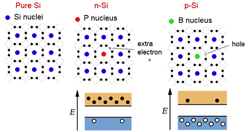
p-type doping: majority carriers are holes.
The technology of integrated circuits:
„Planar” fabrication process: All chips on the surface of the wafer are fabricated simultaneously.
Steps of the fabrication: Semiconductor, metal and insulator layers are deposited onto each other and patterned.
Typical materials to be used:
- Si substrate – doped at the needed areas
- SiO2 layers („high-k”, or „low-k” dielectrics)
- Si3N4 passivating layer
- Polycrystalline Si – gate electrodes
- Metal connections and contacts
- Metal interconnects (Cu or Al)
- PSG (phosphosilicate glass) between interconnect layers
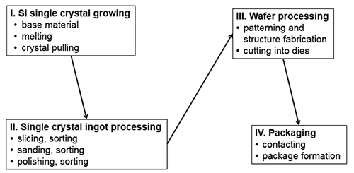
Steps of chip fabrication:
Si single crystal growth:
- Base material: quartz sand (SiO2): Special sand from the Australian coasts due to the strict purity regulation
- Polycrystalline Si fabrication
- Melting poly-Si is is heated up to 1600 °C
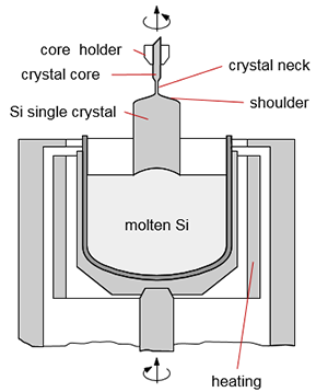
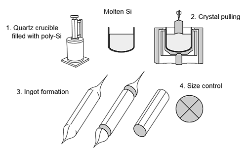
- Ingot pulling: It solidifies from the liquid / molten phase onto a seed seed crystal as a core oriented precisel. Dominant process is the Czochralski-method
Fabrication of polycrystalline Si:
- Raw Si obtained from sand in an arc furnace at high temperature
SiO2 + 2C -> Si + 2CO
Si is still contaminated - Reaction of raw Si with hydrochloric acid
Si + 3HCl ->SiHCl3 + H2
Trichlorosilane gas :easy to be distilled - Deposition of Si from trichlorosilane with CVD process
SiHCl3 + H2 -> Si + 3HCl (at 1000°C)
The silicone created in the last step is deposited from vapor phase onto a Si rod. The clean molten material is made of this rod.
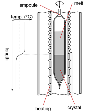
The Czochralski Process:
The oriented seed crystal's rod is very slowly pulled upwards from the melt and rotated at the same time. Important parameters: temperature (melting point: 1414 °C), speed of rotation. Doping can be done from gas or liquid phase. Ingots can be classified according to their purity.
The Bridgman-Strockbager method:
Crystal growth by passing the ampoule through the temperature gradient zone. Not typical for Si.
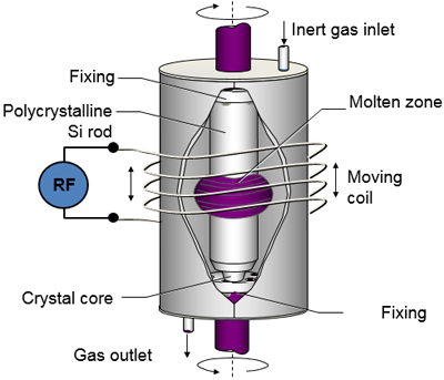
The Floating zone technique:
The polycrystalline rod is molten with a slowly moving induction coil. The slow crystal formation results in a single crystal. The process can be used also for purifying crystals e.g .zone purification. It is based on segregation of different phases.
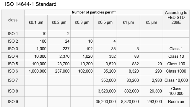
Clean room classification:
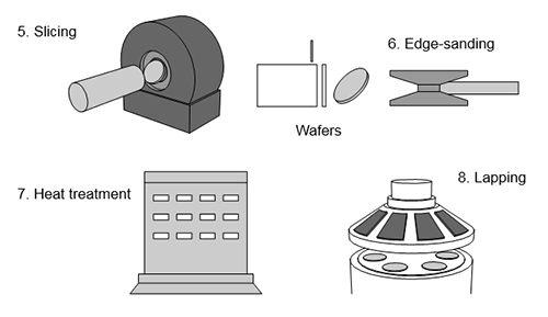
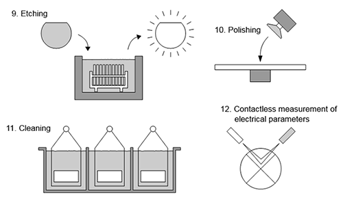
Si single crystal processing steps:
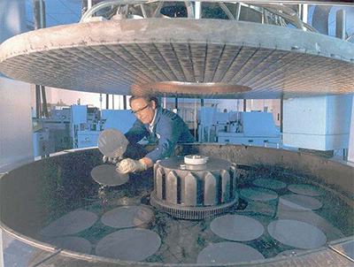
Slicing, Lapping and Polishing:
The silicon ingot is sliced into very thin (~1 mm) wafers with a diamond saw. Slicing causes cracks and contamination on the surface. Multi-step lapping removes the surface silicon which has been cracked or otherwise damaged by the slicing process, and assures a flat surface. Wafers are then etched in a chemically active reagent to remove any crystal damage remained from the previous process steps.
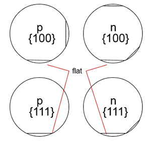
Before slicing: a so called flat cut into the slice, that can be used to denote orientation and doping type.
Lapping is used to remove cracks from the surface; make slices thinner; eliminates mechanical stresses. It results the silicon wafer.
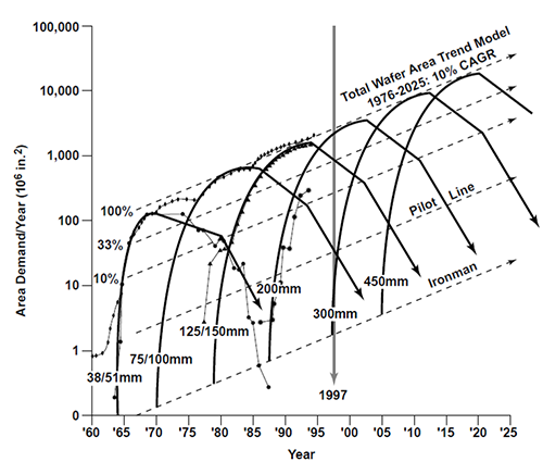
Si wafer size and total wafer area:
Technology is currently shifting from 300mm to 450mm diameter wafer. Total wafer area rises exponentially. Challenges are the large wafer size (large, heavy ingot) and the increasing yield,
From raw Si wafer to device:
- Layer deposition techniques
- Altering conductivity (doping)
- Patterning and structuring (other lecture)
Layer deposition and epitaxy:
Layer deposition: a method to create a universally thin layer (far thinner compared to the lateral size of the substrate) with a large surface area on a substrate. Semiconductors can be patterned with lithography and etching, e.g. interconnections can be created on Si chips. Special case: epitaxy - method of depositing a single-crystal film on a single crystal substrate.
PVD - Physical Vapour Deposition
A method to deposit thin film by the condensation of an evaporized or sputtered material onto the substrate (e.g. Al contact on Si chips). It has two main types: vacuum evaporation and vacuum sputtering. For more detailed description, see „Thin film technologies”. Important! Unlike CVD, there’s no chemical reaction on the surface, therefore this method is more simple.
CVD - Chemical Vapour Deposition
Unlike PVD, chemical reaction occurs on the surface (see lecture „Fabrication of semiconductor wafers, Si deposition”). Raw materials (gases) are often hazardous (explosion, poison hazard, etc.). Common name for the materials: precursor gases. Examples: Si: SiH4 (silane) – flammable, toxic; P: PH3 (phosphine) – flammable, toxic (pest control); B: B2H4 (diborane) - flammable, toxic. The reaction has to be carefully designed in order to avoid reaction between the side products and the wafer.
CVD types:
- APCVD – Atmospheric Pressure CVD: (+) fast, simple, high productivity, (-) less clean method. Application: to grow thick oxide layer.
- LPCVD – Low Pressure CVD: (+) good quality, uniform layer, (-) slow. Application: poly-Si, dielectric layers
- MOCVD – Metallo-Organic CVD (example on the next slide), (+) flexible, several materials (semiconductor, metal, dielectric) can be deposited, (-) highly toxic, hazardous precursors. Application: optical III-V semiconductors, sorts of metallization (Mo, Cu).
- PECVD - Plasma Enhanced CVD: (+) reaction occurs at low temperature due to the presence of plasma, therefore it can be used also after doping (-) plasma can damage the substrate, application: dielectric layers.
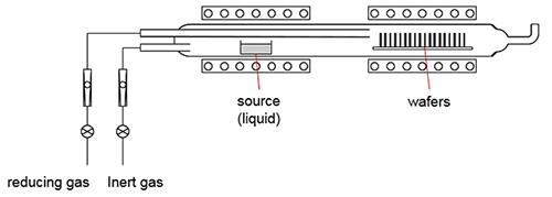
A tipical CVD reactor:
The liquid phase precursor is heated up to its boiling point. Wafers are heated up to the temperature at which CVD reaction occurs. These temperatures are different, so two-zone heating is required. Doping during layer growth can be achieved with the addition of precursors of the dopants.
Materials deposited by CVD:
- Copper – metallization, pads and wiring inside the chip (modern): with MOCVD, common precursor: (hfac)Cu(TMVS) – CupraSelect ® (trademark) metallo-organic material containing copper, it is liquid at room temperature. (Note: Vacuum vaporized aluminum wiring is also used in the case of traditional ICs).
- PSG (phosphosilicate glass), BSG (borosilicate glass) and BPSG (boro-phosphosilicate glass) – dielectrics between metal layers.
- SiO2 (silicon dioxide) – dielectric, used for gate electrodes. TEOS: the reaction of tetra-ethyl- orthosilicate at 600 °C, with diethyl ether formation.
- Si3N4 – insulator layer (provides better protection from H2O molecules and Na ions than SiO2) with PECVD (from the mixture of silane and ammonia).
- Polycrystal silicon – gate electrode, from silane or trichlorosilane.
Epitaxy:
Definition: method of depositing a single-crystal film on a single-crystal substrate. Result: the orientation of the layer and the substrate are (almost) identical. Do not to confuse with thin films and CVD/PVD methods! (Though, epitaxy can also be achieved using CVD as well).
Types of epitaxy:
Homoepitaxy : a crystalline film is grown on a substrate or film of the same material. Ideally, the single-crystal layer is pure and even. Practical application: to grow layers with different doping on the substrate. Homeoepitaxy is the best way to achieve stepped doping profile.
Heteroepitaxy: a crystalline film grows on a crystalline substrate or film of a different material. The difference of lattice constants can not be too large. Application: compound type layer structures for photonic applications (blue, UV laser, laser diodes, vertical cavity lasers) For example: GaN (gallium-nitride) on sapphire substrate, or AlGaInP (Aluminum gallium indium phosphide) on GaAs substrate. SOS: silicon-on –sapphire, e.g. in sensors.
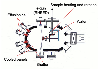
MBE - Molecular Beam Epitaxy
The material is deposited onto the substrate from a slowly evaporating or sublimating source in a controlled way. Requires ultra high vacuum. Good quality layers can be achieved at slow deposition rate. Application: layer structure of modern laser diodes, nanostructures.
The effusion cells (vapor source) are surrounded with liquid N2 -cooled panels (to avoid contamination and to improve vacuum). The molecular beam can be interrupted with a shutter. Layer formation is monitored with reflection high energy electron diffraction (RHEED). The substrate is usually held at 100-300 °C.
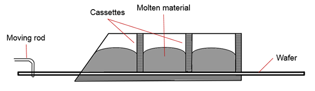
LPE - Liquide Phase Epitaxy
The molten material is deposited from graphite cassettes onto the solid substrate, which is moved under the cassettes. Advantage: fast, simple method (compared to MBE). Application: deposition of layer structures from III-V semiconductor alloys.
VPE - Vapour Phase Epitaxy
The material to be deposited is in vapor phase. VPE is a modification of chemical vapor deposition, in order to grow single-crystal layers. The growth rate of the epitaxial layer highly depends on the composition of the gas. Example: Si growth with VPE, from silicon tetrachloride and hydrogen, at 1200 °C.
Oxide growth on Si
The purpose of growing SiO2: to create a dielectric layer (e.g. gate electrode) and to create a mask layer before diffusion or ion-implantation.
The growth can be done using:
- CVD (see above)
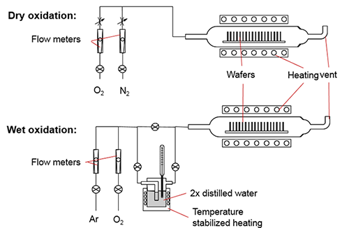
- dry oxidation : Si+O2 -> SiO2; e.g.: at 1000 °C, 7 nm SiO2 can be grown in 15 minutes (gate electrode).
- wet oxidation: Si+2H2O -> SiO2+2H2; e.g.: 10 times faster than dry oxidation. At 1000 °C 700nm SiO2 can be grown in 1,5 hours.
Temperature is typically held between 900-1200 °C. At this temperature H2O and O2 can easily diffuse through silicone-dioxide, so the growth won’t stop.
Doping
Doping concentration can also be changed subsequently (=not during growth, like in homoepitaxy). Two main methods of doping:
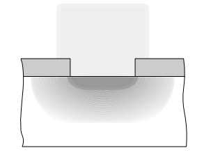
Diffusion: dopant species are present in a solid (thin film) or gaseous form and introduced into the substrate by diffusion.
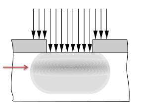
Implantation: direct bombardment of the substrate with highly accelerated ions.
The concentration of the dopant can be calculated/modeled with a function which is not ideal (stepped).
Diffusion: dopant species are present in a solid (thin film) or gaseous form and introduced into the substrate by diffusion.
Implantation: direct bombardment of the substrate with highly accelerated ions.
The concentration of the dopant can be calculated/modeled with a function which is not ideal (stepped).
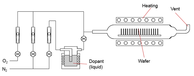
Shematic of a diffusion oven:
Temperature has to be stabilized within an accuracy of ±0,5 °C!
Temperature has to be stabilized within an accuracy of ±0,5 °C!
(Ion) Implantaion
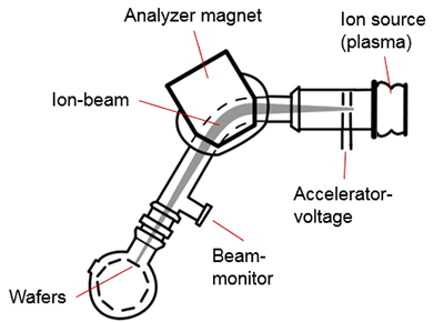
Ion implantation is a process by which dopant materials can be introduced into the substrate in the form of accelerated ions. The penetration depth and the doping profile strongly depends on the energy of the ions, therefore an analyzator magnet is required to choose the ions with the appropriate energy level.
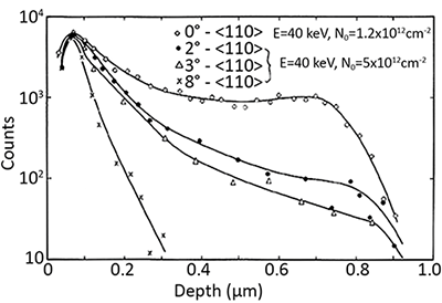
Ion channelling occurs if the direction of ion flow coincides with any low Miller-index orientation of the crystal. At his time, “channels” are formed in the direction of ion flow, where ions tend to collide with each other less probability. The result is that the ion penetration depth is much larger. It has to be avoided during ion implantation, so the substrate has to be oriented a few degrees off-axis. Crystal failures caused by ion implantation can be treated with subsequent heat treatment.
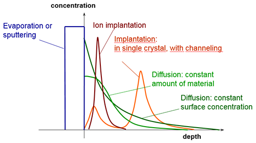
Comparasion of the concentration profiles of diffusion and ion implantation
Diffusion: The surface has the highest concentration.
Implantation:The highest concentration is at a certain depth.
Channeling: occurs in a crystal with a special orientation, it „conducts” the dopant ions. This effect is not preferred, so the substrate is oriented a few degree off-axis.
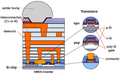
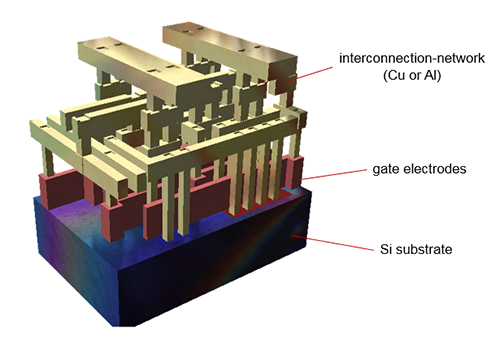
Structure of the modern ICs:
| Previous | Next |