
2- Electronic assembly technologies
2.2 - Reflow soldering technology
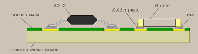
Surface Mount Technology (SMT)
During the process the surface mount devices (SMD) are placed to the specially formed surface of the PWB and joined to the pads mechanically and electrically. The joining technology is usually soldering, sometimes e.g. for heat-sensitive components gluing. The SM devices are available with and without connection leads with solderable surface (Figure 1.). Nowadays the components are: 95% SMD, 5% through hole component.
Passive SM device: the most commonly used types are the chip resistors. These are mostly manufactured by thick film technology to Al2O3 ceramic substrate. The value code (3 characters) is screen printed or laser engraved to the protective glass (value decoding e.g. 683 = 68*103 ohm). The resistor’s dimensions are set with 4 character dimension code. Values of l and d are in 10 mil=254 um.
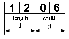
Example: If the dimension code is 1206 than l = 12 x 254 um = 3 mm, d = 6 x 254 um = 1,5 mm.
The dimension codes are usable until 0402. Dimensions for smaller components are: 0402 - 1000x500μm, 0201 - 600x300μm, 01005 - 400x200μm. Nowadays the smallest chip resistor’s dimension code is 01005.
Advantages of surface mounting: smaller size than trugh-hole components while having the same function, greater integration, more functions per area unit, can easily be automated, the components’ package types are standardized, joining technology is usually soldering, rarely conductive adhesive is applied.
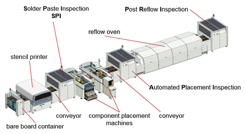
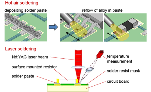
The reflow soldering technology basically consists of three steps; the solder material is in the form of the solder paste:
- deposition of the solder paste by dispensing or by stencil printing
- placement of the components pick&place, collect&place
- remelting the solder alloy in the solder paste – usually in an oven
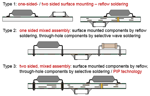
Assembly types of electronic Circuits (prepared by relow soldering)
Solders and Solder pastes
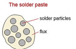
Solder: it is a fusible metal alloy, with a melting point or melting range of 180-300°C, which is melted to join metallic surfaces, especially in the fields of electronics in a process called soldering. The lead-free replacements for conventional Sn60/Pb40 solder have higher melting points, requiring re-engineering of most components and materials used in electronic assemblies. Lead-free solder joints may produce mechanically weaker joints depending on service and manufacture conditions, which may lead to a decrease in reliability using such solders. Solder often comes pre-mixed with, or is used with, flux, a reducing agent designed to help remove impurities (specifically oxidized metals) from the points of contact to improve the electrical connection. For convenience, solder is often manufactured as a hollow tube and filled with flux. In SMT process we use solder paste which is a mix of small solder particles (20-45 um) and flux. It is used extensively in the automated soldering processes reflow soldering.
Solder paste: it is deposited on a printed circuit board by stencil-printing, pneumatic dispensing or pin transfer (where a grid of pins are dipped in solder paste and then applied to the board). The solder particles are frequently a mix of lead-free compounds. Solder paste should be stored in an airtight container at low temperatures (above freezing) but should be warmed to room temperature for use. Different solder pastes are distinguished mainly by the type of flux and metal that is used to make it up and by the relative proportions of these components.
Lead-free solder paste alloys:
| 96.5Sn3Ag0.5Cu | Tin-Silver-Copper | melting temp. 217°C |
|---|---|---|
| 96.5Sn3.5Ag | Tin-Silver | melting temp. 221°C |
| 99.3Sn0.7Cu | Tin-Copper paste | melting temp. 227°C |
Conventional leaded solder paste alloys:
| 63Sn37Pb | eutectic Tin-Lead | melting temp. 187°C |
|---|---|---|
| 60Sn40Pb | Tin-Lead | melting temp. 188°C |
| 62Sn36Pb2Ag | Tin-Lead-Silver | melting temp. 179°C |
The Restriction of Hazardous Substances Directive (RoHS) 2002/95/EC was adopted in February 2003 by the European Union. The RoHS directive took effect on July 1, 2006. This directive restricts the use of six hazardous materials in the manufacture of various types of electronic and electrical equipment.
Solder materials:
Solder paste: suspension containing solder powder and flux, typical diameter of solder particles is 20…45 μm; metal content 85…91 wt%
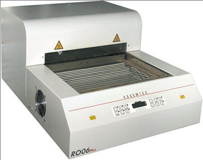
 Stencil printing
Type of solder pastes
| Pitch | Diameter of solder particle >90% |
Diameter of solder particle <1% bigger |
|
|---|---|---|---|
| Type 1 | 1 mm | 150 µm…75 µm | 150 µm |
| Type 2 | 0.63 mm | 75 µm... 45 µm | 75 µm |
| Type 3 | 0.5 mm | 45 µm…25 µm | 45 µm |
| Type 4 | 0.4 mm | 38 µm…20 µm | 38 µm |
| Type 5 | 0.3 mm | 25 µm…15 µm | 25 µm |
| Type 6 | 0.2 mm | 15 µm...5 µm | 15 µm |
Solder preforms: shape is formed according to component leads to be soldered (e.g. caps of metal packages, leadframes); solder deposition is easier
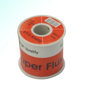
Flux core solder wire: used during hand soldering or for the rework of soldering defects; typical wire diameter 0.3…1.8 mm
Solder bars: used for wave soldering
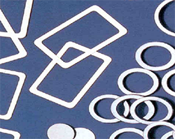
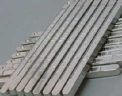
Stencil printing The stencil applied for depositing the solder paste is a thin, 75–200 µm thick metal foil, on which apertures are formed according to the solder pads on the printed circuit board. Stencil printing provides a fast, mass solder paste deposition process; relatively expensive, appropriate and recommended for mass production.
Animáció!
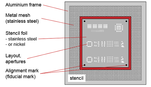
Build-up of Stencils (Terms)
The stencil foil is tensioned and fixed to the frame by a metal mesh. The tension of stencil foil is around ~ 50 N/cm.
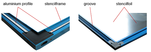
Vectorguard stencilframes:
In the Vectorguard stencil frame, springs tighten aluminium profiles, which cling into the grooves formed along the edges of the stencil foil. Ahead of the springs there is a silicon tube. By blowing up the tube with compressed air, the profiles open and the stencil foil can be inserted into the frame. By deflating the tube, the profiles close and the stencil foil becomes tight.
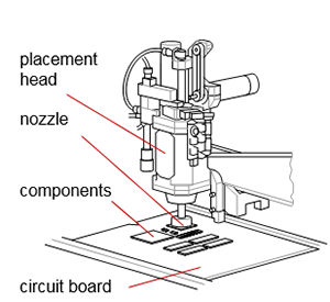
Component Placement
Classification by level of automation: manual, semi-automatic, automatic
Classification by the type of placement head: pick&place, collect&place
The process:
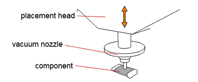
1. Pick a component with a vacuum nozle from a feeder (tape, tray)), the size of the vacuum nozzle is variable according to the size of the component.
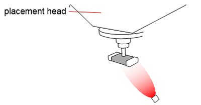
2. Measuring the position of the component on the nozzle – correcting placement coordinate (measuring with laser beam or optical camera)
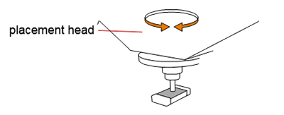
3. Rotating the component to proper orientation , correcting the angular offset
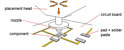
4. Positioning the component , to its location on the circuit board, placing the component into the solder paste (in the case of wave soldering, into the adhesive)
Types of the Placement heads:
Pick & place: slow, very accurate machines; for fine-pitch IC placement; speed: ~ 14.000 comp./hours
Collect & place: fast, less accurate machines; for small (mainly passive) SMD placement; speed: ~ 40.000–90.000 comp./hours
Pick-and-Place machines:
- Manual pick-and-place machine: picks a component from the feeder, then placing it manually to the PWB one at a time.
- Automatic pick-and-place machine: picks a component from the feeder, then placing it to the PWB according to the CAD program.
- Collect-and-place machine: collects several components from the feeder, then placing them to the PWB according to the CAD program.
Reflow soldering
Reflow oven types:
Batch type oven:
- mainly infrared radiation is used for heating
- only 1 zone
- small size
- offline equipment
- low productivity
- appropriate for small batches, laboratory works
Conveyor type oven:
- the assembly goes through different temperature zones on a conveyor
- heating zones are adjustable
- the thermal profile is determined by the zone temperatures and the conveyor speed
- 3–12 zones
- mostly forced convection is used for heat transfer
- the assembly travels through separate heating and cooling zones
- the temperatures of the zones are individually adjustable
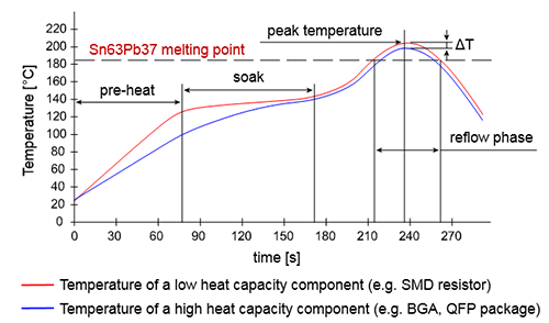
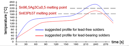
Temperature profiles of the relfow soldering:
| Profile phase | lead-bearing solder | lead-free solder |
|---|---|---|
| Ramp | Temperature range: 0-120 °C Temperature gradient: <2 °C/s Time spent in this phase: 60-150 |
Temperature range: 0-150 °C Temperature gradient: 2-4 °C/s Time spent in this phase: 60-150 s |
| Soak | Temperature range: 120-150 °C Time spent in this phase: 60-90 s |
Temperature range: 150-190 °C Time spent in this phase: 60-120 s |
| Reflow | Peak temperature: 205-230 °C Time spent in this phase: 45-90 s |
Peak temperature: 230-255 °C Time spent in this phase: 20-60 s |
| Cooling down | Cool down to 130 °C Temperature gradient: 3-4 °C/s |
Cool down to 130 °C Temperature gradient: 4-5 °C/s |
The lead-free solders and the joining higher temperature profile causes problems. As the fig.9. shows the lead-free profile could be 20-30 °C higher than the Sn-Pb profile. The pre-heating and soaking time also longer. This higher temperature at longer period could affect the different components (plastic package, BGA).
Common error reflow failures: skewing, tombstoning, formation of solder balls and beads near to the soldering positions, void formation inside the solder, bridging, open joints.
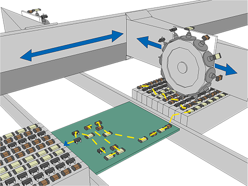
Production line for reflow soldering technology:
Other relfow soldering technology:
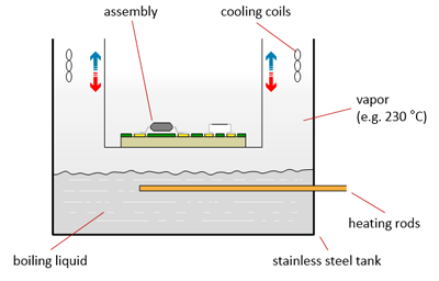
Vapour Phase Soldering:
The principle of vapour phase soldering is using the heat transfer effect of condensation. During the process a special heat transfer fluid is heated at the bottom of a tank. When the fluid is heated up to its boiling point, a vapour space begins developing which fill up a closed tank. The excessive vapour is condensed on the top of the tank, due to a cooling pipe setup. When the vapour space is ready for soldering, the assembled PCB is immersed into the vapour, and a condensate layer forms on the colder surface of the PCB. This layer transfers the latent heat of condensing mass and the conducted heat from surrounding vapour to the assembly, which is heated up to the boiling point of the heat transfer fluid. After a while, the PCB is lifted out of the process zone in order to cool down, and to solidify the melted alloy. Nowadays the most widely applied heat transfer fluid is Galden, which contains ether chains closed with carbon-fluorine bonds (Perfluoropolyether, PFPE). The boiling point of the Galden liquid can be set with the length of the ether chai between 150 and 240 ºC.
| Previous | Next |